SNAS365G May 2006 – June 2016 DAC082S085
PRODUCTION DATA.
- 1 Features
- 2 Applications
- 3 Description
- 4 Revision History
- 5 Description (continued)
- 6 Pin Configuration and Functions
- 7 Specifications
- 8 Detailed Description
- 9 Application and Implementation
- 10Power Supply Recommendations
- 11Layout
- 12Device and Documentation Support
- 13Mechanical, Packaging, and Orderable Information
封装选项
机械数据 (封装 | 引脚)
散热焊盘机械数据 (封装 | 引脚)
- DSC|10
订购信息
1 Features
- Ensured Monotonicity
- Low Power Operation
- Rail-to-Rail Voltage Output
- Power-On Reset to 0 V
- Simultaneous Output Updating
- Wide Power Supply Range: 2.7 V to 5.5 V
- Industry's Smallest Package
- Power-Down Modes
- Key Specifications:
- Resolution: 8 Bits
- INL: ±0.5 LSB (Maximum)
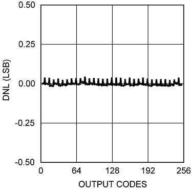
- DNL: 0.18 / –0.13 LSB (Maximum)
- Settling Time: 4.5 µs (Maximum)
- Zero Code Error: 15 mV (Maximum)
- Full-Scale Error: –0.75% FS (Maximum)
- Supply Power:
- Normal: 0.6 mW (3 V) / 1.6 mW (5 V) (Typical)
- Power Down: 0.3 µW (3 V) / 0.8 µW (5 V) (Typical)
2 Applications
3 Description
The DAC082S085 device is a full-featured, general-purpose, DUAL, 8-bit, voltage-output, digital-to-analog converter (DAC) that can operate from a single 2.7-V to 5.5-V supply and consumes 0.6 mW at 3 V and 1.6 mW at 5 V. The DAC082S085 is packaged in 10-pin SON and VSSOP packages. The 10-pin WSON package makes the DAC082S085 the smallest DUAL DAC in its class. The on-chip output amplifier allows rail-to-rail output swing, and the three-wire serial interface operates at clock rates up to 40 MHz over the entire supply voltage range. Competitive devices are limited to 25-MHz clock rates at supply voltages in the 2.7 V to 3.6 V range. The serial interface is compatible with standard SPI™, QSPI, MICROWIRE, and DSP interfaces.
Device Information(1)
| PART NUMBER | PACKAGE | BODY SIZE (NOM) |
|---|---|---|
| DAC082S085 | VSSOP (10) | 3.00 mm × 3.00 mm |
| WSON (10) | 3.00 mm × 3.00 mm |
- For all available packages, see the orderable addendum at the end of the data sheet.
DNL at VA = 3 V
