SNAS363F May 2006 – March 2016 DAC084S085
PRODUCTION DATA.
- 1 Features
- 2 Applications
- 3 Description
- 4 Revision History
- 5 Description
- 6 Pin Configuration and Functions
- 7 Specifications
- 8 Detailed Description
- 9 Application and Implementation
- 10Power Supply Recommendations
- 11Layout
- 12Device and Documentation Support
- 13Mechanical, Packaging, and Orderable Information
封装选项
机械数据 (封装 | 引脚)
散热焊盘机械数据 (封装 | 引脚)
- DSC|10
订购信息
9 Application and Implementation
NOTE
Information in the following applications sections is not part of the TI component specification, and TI does not warrant its accuracy or completeness. TI’s customers are responsible for determining suitability of components for their purposes. Customers should validate and test their design implementation to confirm system functionality.
9.1 Application Information
9.1.1 Bipolar Operation
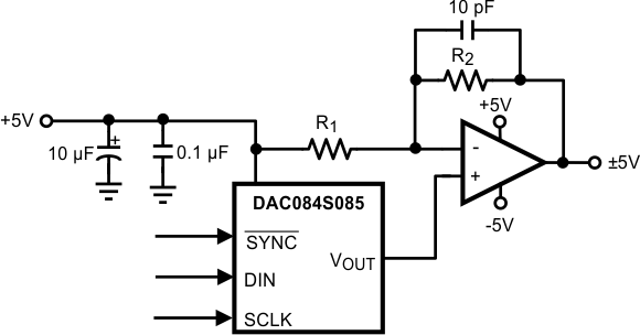
The DAC084S085 is designed for single-supply operation and thus has a unipolar output. However, a bipolar output may be obtained with the circuit in Figure 35. This circuit provides an output voltage range of ±5 V. A rail-to-rail amplifier must be used if the amplifier supplies are limited to ±5 V.
 Figure 35. Bipolar Operation
The output voltage of this circuit for any code is found to be:
where
- D is the input code in decimal form.
With VA = 5 V and R1 = R2,
A list of rail-to-rail amplifiers suitable for this application are indicated in Table 2.
Table 2. Some Rail-to-Rail Amplifiers
| AMP | PKGS | Typ VOS | Typ ISUPPLY |
|---|---|---|---|
| LMC7111 | DIP-8 SOT23-5 |
0.9 mV | 25 µA |
| LM7301 | SO-8 SOT23-5 |
0.03 mV | 620 µA |
| LM8261 | SOT23-5 | 0.7 mV | 1 mA |
9.2 Typical Application
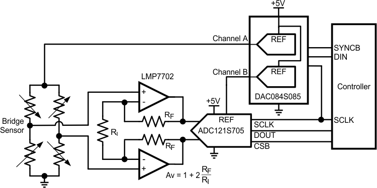
 Figure 36. Driving an ADC Reference
9.2.1 Design Requirements
Figure 36 shows Channel A of the DAC084S085 providing the drive or supply voltage for a bridge sensor. By having the sensor supply voltage adjustable, the output of the sensor can be optimized to the input level of the ADC monitoring it.
9.2.2 Detailed Design Procedure
The output of the sensor is amplified by a fixed gain amplifier stage with a differential gain of 1 + 2 × (RF / RI). The advantage of this amplifier configuration is the high input impedance seen by the output of the bridge sensor. The disadvantage is the poor common-mode rejection ratio (CMRR). The common-mode voltage (VCM) of the bridge sensor is half of DAC output of Channel A. The VCM is amplified by a gain of 1 V/V by the amplifier stage and thus becomes the bias voltage for the input of the ADC121S705. Channel B of the DAC084S085 is providing the reference voltage to the ADC121S705. The reference for the ADC121S705 may be set to any voltage from 1 V to 5 V, providing the widest dynamic range possible.
The reference voltage for Channel A and B is powered by an external 5-V power supply. Because the 5-V supply is common to the sensor supply voltage and the reference voltage of the ADC, fluctuations in the value of the
5-V supply has a minimal effect on the digital output code of the ADC. This type of configuration is often referred to as a ratiometric design. For example, an increase of 5% to the 5-V supply causes the sensor supply voltage to increase by 5%. This causes the gain or sensitivity of the sensor to increase by 5%. The gain of the amplifier stage is unaffected by the change in supply voltage. The ADC121S705 on the other hand, also experiences a 5% increase to its reference voltage. This causes the size of the ADC's least significant bit (LSB) to increase by 5%. As a result of the gain of the sensor increasing by 5% and the LSB size of the ADC increasing by the same 5%, there is no net effect on the circuit's performance. It is assumed that the amplifier gain is set low enough to allow for a 5% increase in the sensor output. Otherwise, the increase in the sensor output level may cause the output of the amplifiers to clip.
9.2.3 Application Curve
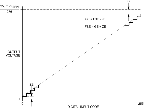
 Figure 37. Input / Output Transfer Characteristic