SNAS424D August 2007 – April 2016 DAC088S085
PRODUCTION DATA.
- 1 Features
- 2 Applications
- 3 Description
- 4 Revision History
- 5 Description (continued)
- 6 Pin Configuration and Functions
- 7 Specifications
- 8 Detailed Description
- 9 Application and Implementation
- 10Power Supply Recommendations
- 11Layout
- 12Device and Documentation Support
- 13Mechanical, Packaging, and Orderable Information
封装选项
机械数据 (封装 | 引脚)
散热焊盘机械数据 (封装 | 引脚)
- RGH|16
订购信息
8 Detailed Description
8.1 Overview
The DAC085S085 is fabricated on a CMOS process with an architecture that consists of switches and resistor strings that are followed by an output buffer.
8.2 Functional Block Diagram

8.3 Feature Description
8.3.1 DAC Architecture
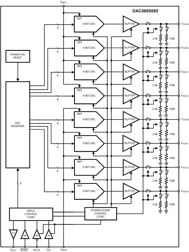
The DAC088S085 is fabricated on a CMOS process with an architecture that consists of switches and resistor strings that are followed by an output buffer. The reference voltages are externally applied at VREF1 for DAC channels A through D and VREF2 for DAC channels E through H.
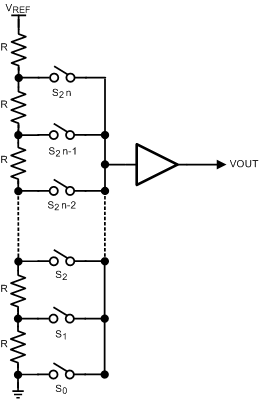
For simplicity, a single resistor string is shown in Figure 27. This string consists of 256 equal valued resistors with a switch at each junction of two resistors, plus a switch-to-ground. The code loaded into the DAC register determines which switch is closed, connecting the proper node to the amplifier. The input coding is straight binary with an ideal output voltage of:
where
- D is the decimal equivalent of the binary code that is loaded into the DAC register.
D can take on any value between 0 and 255. This configuration ensures that the DAC is monotonic.
 Figure 27. DAC Resistor String
Because all eight DAC channels of the DAC088S085 can be controlled independently, each channel consists of a DAC register and a 8-bit DAC. Figure 28 is a simple block diagram of an individual channel in the DAC088S085. Depending on the mode of operation, data written into a DAC register causes the 8-bit DAC output to be updated or an additional command is required to update the DAC output. Further description of the modes of operation can be found in Serial Interface.
 Figure 28. Single-Channel Block Diagram
8.3.2 Output Amplifiers
The output amplifiers are rail-to-rail, providing an output voltage range of 0 V to VA when the reference is VA. All amplifiers, even rail-to-rail types, exhibit a loss of linearity as the output approaches the supply rails (0 V and VA, in this case). For this reason, linearity is specified over less than the full output range of the DAC. However, if the reference is less than VA, there is only a loss in linearity in the lowest codes.
The output amplifiers are capable of driving a load of 2 kΩ in parallel with 1500 pF to ground or to VA. The zero-code and full-scale outputs for given load currents are available in Electrical Characteristics.
8.3.3 Reference Voltage
The DAC088S085 uses dual external references, VREF1 and VREF2, that are shared by channels A, B, C, D and channels E, F, G, H respectively. The reference pins are not buffered and have an input impedance of 30 kΩ. TI recommends that VREF1 and VREF2 be driven by voltage sources with low output impedance. The reference voltage range is 0.5 V to VA, providing the widest possible output dynamic range.
8.4 Device Functional Modes
8.4.1 Power-On Reset
The power-on reset circuit controls the output voltages of the eight DACs during power up. Upon application of power, the DAC registers are filled with zeros and the output voltages are set to 0 V. The outputs remain at 0 V until a valid write sequence is made.
8.4.2 Power-Down Modes
The DAC088S085 has three power-down modes where different output terminations can be selected (see Table 1). With all channels powered down, the supply current drops to 0.1 µA at 3 V and 0.2 µA at 5 V. By selecting the channels to be powered down in DB[7:0] with a 1, individual channels can be powered down separately or multiple channels can be powered down simultaneously. The three different output terminations include high output impedance, 100 kΩ to GND, and 2.5 kΩ to GND.
The output amplifiers, resistor strings, and other linear circuitry are all shut down in any of the power-down modes. The bias generator, however, is only shut down if all the channels are placed in power down mode. The contents of the DAC registers are unaffected when in power down. Therefore, each DAC register maintains its value before the DAC088S085 being powered down unless it is changed during the write sequence which instructed it to recover from power down. Minimum power consumption is achieved in the power-down mode with SYNC idled high, DIN idled low, and SCLK disabled. The time to exit power-down (Wake-Up Time) is typically 3 µs at 3 V and 20 µs at 5 V.
Table 1. Power-Down Modes
| DB[15:12] | DB[11:8] | 7 | 6 | 5 | 4 | 3 | 2 | 1 | 0 | OUTPUT IMPEDANCE |
|---|---|---|---|---|---|---|---|---|---|---|
| 1 1 0 1 | X X X X | H | G | F | E | D | C | B | A | High-Z outputs |
| 1 1 1 0 | X X X X | H | G | F | E | D | C | B | A | 100-kΩ outputs |
| 1 1 1 1 | X X X X | H | G | F | E | D | C | B | A | 2.5-kΩ outputs |
8.5 Programming
8.5.1 Serial Interface
The three-wire interface is compatible with SPI, QSPI, and MICROWIRE, as well as most DSPs and operates at clock rates up to 40 MHz. A valid serial frame contains 16 falling edges of SCLK. See Figure 1 for information on a write sequence.
A write sequence begins by bringing the SYNC line low. Once SYNC is low, the data on the DIN line is clocked into the 16-bit serial input register on the falling edges of SCLK. To avoid mis-clocking data into the shift register, it is critical that SYNC not be brought low on a falling edge of SCLK (see minimum and maximum setup times for SYNC in Figure 1 and Figure 29). On the 16th falling edge of SCLK, the last data bit is clocked into the register. The write sequence is concluded by bringing the SYNC line high. Once SYNC is high, the programmed function (a change in the DAC channel address, mode of operation or register contents) is executed. To avoid mis-clocking data into the shift register, it is critical that SYNC be brought high between the 16th and 17th falling edges of SCLK (see minimum and maximum hold times for SYNC in Figure 1 and Figure 29).
 Figure 29. CS Setup and Hold Times
If SYNC is brought high before the 15th falling edge of SCLK, the write sequence is aborted and the data that has been shifted into the input register is discarded. If SYNC is held low beyond the 17th falling edge of SCLK, the serial data presented at DIN begins to be output on DOUT. More information on this mode of operation can be found in Daisy Chain Operation. In either case, SYNC must be brought high for the minimum specified time before the next write sequence is initiated with a falling edge of SYNC.
Because the DIN buffer draws more current when it is high, it must be idled low between write sequences to minimize power consumption. On the other hand, SYNC must be idled high to avoid the activation of daisy chain operation where DOUT is active.
8.5.2 Daisy Chain Operation
Daisy chain operation allows communication with any number of DAC088S085s using a single serial interface. As long as the correct number of data bits are input in a write sequence (multiple of sixteen bits), a rising edge of SYNC properly updates all DACs in the system.
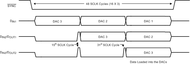
To support multiple devices in a daisy chain configuration, SCLK and SYNC are shared across all DAC088S085s and DOUT of the first DAC in the chain is connected to DIN of the second. Figure 30 shows three DAC088S085s connected in daisy chain fashion. Similar to a single-channel write sequence, the conversion for a daisy chain operation begins on a falling edge of SYNC and ends on a rising edge of SYNC. A valid write sequence for n devices in a chain requires n times 16 falling edges to shift the entire input data stream through the chain. Daisy chain operation is specified for a maximum SCLK speed of 30 MHz.
 Figure 30. Daisy Chain Configuration
The serial data output pin, DOUT, is available on the DAC088S085 to allow daisy-chaining of multiple DAC088S085 devices in a system. In a write sequence, DOUT remains low for the first fourteen falling edges of SCLK before going high on the fifteenth falling edge. Subsequently, the next sixteen falling edges of SCLK outputs the first sixteen data bits entered into DIN. Figure 31 shows the timing of three DAC088S085s in Figure 30. In this instance, It takes forty-eight falling edges of SCLK followed by a rising edge of SYNC to load all three DAC088S085s with the appropriate register data. On the rising edge of SYNC, the programmed function is executed in each DAC088S085 simultaneously.
 Figure 31. Daisy Chain Timing Diagram
8.5.3 Serial Input Register
The DAC088S085 has two modes of operation plus a few special command operations. The two modes of operation are Write Register Mode (WRM) and Write Through Mode (WTM). For the rest of this document, these modes is referred to as WRM and WTM. The special command operations are separate from WRM and WTM because they can be called upon regardless of the current mode of operation. The mode of operation is controlled by the first four bits of the control register, DB15 through DB12. See Table 2 for a detailed summary.
Table 2. Write Register and Write Through Modes
| DB[15:12] | DB[11:0] | DESCRIPTION OF MODE |
|---|---|---|
| 1 0 0 0 | X X X X X X X X X X X X | WRM: The registers of each DAC Channel can be written to without causing their outputs to change. |
| 1 0 0 1 | X X X X X X X X X X X X | WTM: Writing data to a channel's register causes the DAC output to change. |
When the DAC088S085 first powers up, the DAC is in WRM. In WRM, the registers of each individual DAC channel can be written to without causing the DAC outputs to be updated. This is accomplished by setting DB15 to 0, specifying the DAC register to be written to in DB[14:12], and entering the new DAC register setting in DB[11:0] (see Table 3).The DAC088S085 remains in WRM until the mode of operation is changed to WTM. The mode of operation is changed from WRM to WTM by setting DB[15:12] to 1001. Once in WTM, writing data to a DAC channel's register causes the DAC's output to be updated as well. Changing a DAC channel's register in WTM is accomplished in the same manner as it is done in WRM. However, in WTM the DAC's register and output are updated at the completion of the command (see Table 3). Similarly, the DAC088S085 remains in WTM until the mode of operation is changed to WRM by setting DB[15:12] to 1000.
Table 3. Commands Impacted by WRM and WTM
| DB15 | DB[14:12] | DB[11:0] | DESCRIPTION OF MODE |
|---|---|---|---|
| 0 | 0 0 0 | D11 D10 ... D4 X X X X | WRM: D[11:0] written to ChA's data register only WTM: ChA's output is updated by data in D[11:0] |
| 0 | 0 0 1 | D11 D10 ... D4 X X X X | WRM: D[11:0] written to ChB's data register only WTM: ChB's output is updated by data in D[11:0] |
| 0 | 0 1 0 | D11 D10 ... D4 X X X X | WRM: D[11:0] written to ChC's data register only WTM: ChC's output is updated by data in D[11:0] |
| 0 | 0 1 1 | D11 D10 ... D4 X X X X | WRM: D[11:0] written to ChD's data register only WTM: ChD's output is updated by data in D[11:0] |
| 0 | 1 0 0 | D11 D10 ... D4 X X X X | WRM: D[11:0] written to ChE's data register only WTM: ChE's output is updated by data in D[11:0] |
| 0 | 1 0 1 | D11 D10 ... D4 X X X X | WRM: D[11:0] written to ChF's data register only WTM: ChF's output is updated by data in D[11:0] |
| 0 | 1 1 0 | D11 D10 ... D4 X X X X | WRM: D[11:0] written to ChG's data register only WTM: ChG's output is updated by data in D[11:0] |
| 0 | 1 1 1 | D11 D10 ... D4 X X X X | WRM: D[11:0] written to ChH's data register only WTM: ChH's output is updated by data in D[11:0] |
As mentioned previously, the special command operations can be exercised at any time regardless of the mode of operation. There are three special command operations. The first command is exercised by setting data bits DB[15:12] to 1010. This allows a user to update multiple DAC outputs simultaneously to the values currently loaded in their respective control registers. This command is valuable if the user wants each DAC output to be at a different output voltage but still have all the DAC outputs change to their appropriate values simultaneously (see Table 4).
The second special command allows the user to alter the DAC output of channel A with a single write frame. This command is exercised by setting data bits DB[15:12] to 1011 and data bits DB[11:0] to the desired control register value. It also has the added benefit of causing the DAC outputs of the other channels to update to their current control register values as well. A user may choose to exercise this command to save a write sequence. For example, the user may wish to update several DAC outputs simultaneously, including channel A. To accomplish this task in the minimum number of write frames, the user would alter the control register values of all the DAC channels except channel A while operating in WRM. The last write frame would be used to exercise the special command Channel A Write Mode. In addition to updating channel A's control register and output to a new value, all of the other channels would be updated as well. At the end of this sequence of write frames, the DAC088S085 would still be operating in WRM (see Table 4).
The third special command allows the user to set all the DAC control registers and outputs to the same level. This command is commonly referred to as broadcast mode because the same data bits are being broadcast to all of the channels simultaneously. This command is exercised by setting data bits DB[15:12] to 1100 and data bits DB[7:0] to the value that the user wishes to broadcast to all the DAC control registers. Once the command is exercised, each DAC output is updated by the new control register value. This command is frequently used to set all the DAC outputs to some known voltage such as 0 V, VREF / 2, or Full Scale. A summary of the commands can be found in Table 4.
Table 4. Special Command Operations
| DB[15:12] | DB[11:0] | DESCRIPTION OF MODE |
|---|---|---|
| 1 0 1 0 | X X X X H G F E D C B A | Update Select: The DAC outputs of the channels selected with a 1 in DB[7:0] are updated simultaneously to the values in their respective control registers. |
| 1 0 1 1 | D11 D10 ... D4 X X X X | Channel A Write: the control register of Channel A and DAC output are updated to the data in DB[11:0]. The outputs of the other seven channels are also updated according to their respective control register values. |
| 1 1 0 0 | D11 D10 ... D4 X X X X | Broadcast: The data in DB[11:0] is written to all channels' control register and DAC output simultaneously. |