SNAS424D August 2007 – April 2016 DAC088S085
PRODUCTION DATA.
- 1 Features
- 2 Applications
- 3 Description
- 4 Revision History
- 5 Description (continued)
- 6 Pin Configuration and Functions
- 7 Specifications
- 8 Detailed Description
- 9 Application and Implementation
- 10Power Supply Recommendations
- 11Layout
- 12Device and Documentation Support
- 13Mechanical, Packaging, and Orderable Information
封装选项
机械数据 (封装 | 引脚)
散热焊盘机械数据 (封装 | 引脚)
- RGH|16
订购信息
7 Specifications
7.1 Absolute Maximum Ratings
over operating free-air temperature range (unless otherwise noted)(1)(2)(5)| MIN | MAX | UNIT | |
|---|---|---|---|
| Supply voltage, VA | 6.5 | V | |
| Voltage on any input pin | –0.3 | 6.5 | V |
| Input current at any pin(3) | 10 | mA | |
| Package input current(3) | 30 | mA | |
| Power Consumption at TA = 25°C | See(4) | ||
| Junction temperature, TJ | 150 | °C | |
| Storage temperature, Tstg | –65 | 150 | °C |
(1) Stresses beyond those listed under Absolute Maximum Ratings may cause permanent damage to the device. These are stress ratings only, which do not imply functional operation of the device at these or any other conditions beyond those indicated under Recommended Operating Conditions. Exposure to absolute-maximum-rated conditions for extended periods may affect device reliability.
(2) All voltages are measured with respect to GND = 0 V, unless otherwise specified.
(3) When the input voltage at any pin exceeds 5.5 V or is less than GND, the current at that pin must be limited to 10 mA. The 30-mA maximum package input current rating limits the number of pins that can safely exceed the power supplies with an input current of 10 mA to three.
(4) The absolute maximum junction temperature (TJmax) for this device is 150°C. The maximum allowable power dissipation is dictated by TJmax, the junction-to-ambient thermal resistance (RθJA), and the ambient temperature (TA), and can be calculated using the formula PDMAX = (TJmax – TA) / RθJA. The values for maximum power dissipation is reached only when the device is operated in a severe fault condition (for example, when input or output pins are driven beyond the operating ratings, or the power supply polarity is reversed). Such conditions must always be avoided.
(5) If Military/Aerospace specified devices are required, please contact the Texas Instruments Sales Office/Distributors for availability and specifications.
7.2 ESD Ratings
| VALUE | UNIT | |||
|---|---|---|---|---|
| V(ESD) | Electrostatic discharge | Human-body model (HBM), per ANSI/ESDA/JEDEC JS-001(1) | ±2500 | V |
| Charged-device model (CDM), per JEDEC specification JESD22-C101(2) | ±1000 | |||
| Machine model (MM) | ±250 | |||
(1) JEDEC document JEP155 states that 500 V HBM allows safe manufacturing with a standard ESD control process.
(2) JEDEC document JEP157 states that 250 V CDM allows safe manufacturing with a standard ESD control process.
7.3 Recommended Operating Conditions
over operating free-air temperature range (unless otherwise noted)(1)| MIN | MAX | UNIT | |
|---|---|---|---|
| Operating temperature, TA | –40 | 125 | °C |
| Supply voltage, VA | 2.7 | 5.5 | V |
| Reference voltage, VREF1,2 | 0.5 | VA | V |
| Digital input voltage(2) | 0 | 5.5 | V |
| Output load | 0 | 1500 | pF |
| SCLK frequency | 40 | MHz |
(1) All voltages are measured with respect to GND = 0 V, unless otherwise specified.
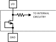
(2) The inputs are protected as shown below. Input voltage magnitudes up to 5.5 V, regardless of VA, does not cause errors in the conversion result. For example, if VA is 3 V, the digital input pins can be driven with a 5 V logic device.

7.4 Thermal Information
| THERMAL METRIC(1)(2) | DAC088S085 | UNIT | ||
|---|---|---|---|---|
| PW (TSSOP) | RGH (WQFN) | |||
| 16 PINS | 16 PINS | |||
| RθJA | Junction-to-ambient thermal resistance | 130 | 38 | °C/W |
| RθJC(top) | Junction-to-case (top) thermal resistance | 32 | 21 | °C/W |
| RθJB | Junction-to-board thermal resistance | 44.2 | 9.8 | °C/W |
| ψJT | Junction-to-top characterization parameter | 2 | 0.2 | °C/W |
| ψJB | Junction-to-board characterization parameter | 43.5 | 9.8 | °C/W |
| RθJC(bot) | Junction-to-case (bottom) thermal resistance | — | 2.4 | °C/W |
(1) For more information about traditional and new thermal metrics, see the Semiconductor and IC Package Thermal Metrics application report, SPRA953.
(2) Soldering process must comply with Texas Instruments' Reflow Temperature Profile specifications. See http://www.ti.com/packaging. Reflow temperature profiles are different for lead-free packages.
7.5 Electrical Characteristics
The following specifications apply for VA = 2.7 V to 5.5 V, VREF1 = VREF2 = VA, CL = 200 pF to GND, fSCLK = 30 MHz, input code range 3 to 252. Typical values apply for TA = 25°C; minimum and maximum limits apply for TA = –40°C to 125°C, unless otherwise specified.| PARAMETER | TEST CONDITIONS | MIN | TYP | MAX | UNIT | ||
|---|---|---|---|---|---|---|---|
| STATIC PERFORMANCE | |||||||
| Resolution | 8 | Bits | |||||
| Monotonicity | 8 | Bits | |||||
| INL | Integral non‑linearity | ±0.12 | ±0.5 | LSB | |||
| DNL | Differential non‑linearity | 0.03 | 0.15 | LSB | |||
| –0.1 | –0.02 | ||||||
| ZE | Zero code error | IOUT = 0 | 5 | 15 | mV | ||
| FSE | Full-scale error | IOUT = 0 | –0.1 | –0.75 | %FSR | ||
| GE | Gain error | –0.2 | –1 | %FSR | |||
| ZCED | Zero code error drift | –20 | µV/°C | ||||
| TC GE | Gain error tempco | –1 | ppm/°C | ||||
| OUTPUT CHARACTERISTICS | |||||||
| Output voltage range | 0 | VREF1,2 | V | ||||
| IOZ | High-impedance output leakage current(1) | ±1 | µA | ||||
| ZCO | Zero code output | VA = 3 V, IOUT = 200 µA | 10 | mV | |||
| VA = 3 V, IOUT = 1 mA | 45 | ||||||
| VA = 5 V, IOUT = 200 µA | 8 | ||||||
| VA = 5 V, IOUT = 1 mA | 34 | ||||||
| FSO | Full scale output | VA = 3 V, IOUT = 200 µA | 2.984 | V | |||
| VA = 3 V, IOUT = 1 mA | 2.933 | ||||||
| VA = 5 V, IOUT = 200 µA | 4.987 | ||||||
| VA = 5 V, IOUT = 1 mA | 4.955 | ||||||
| IOS | Output short circuit current (source) | VA = 3 V, VOUT = 0 V, Input Code = FFh | –50 | mA | |||
| VA = 5 V, VOUT = 0 V, Input Code = FFh | –60 | ||||||
| IOS | Output short circuit current (sink) | VA = 3 V, VOUT = 3 V, Input Code = 00h | 50 | mA | |||
| VA = 5 V, VOUT = 5 V, Input Code = 00h | 70 | ||||||
| IO | Continuous output current per channel(1) | TA = 105°C | 10 | mA | |||
| TA = 125°C | 6.5 | ||||||
| CL | Maximum load capacitance | RL = ∞ | 1500 | pF | |||
| RL = 2 kΩ | 1500 | ||||||
| ZOUT | DC output impedance | 8 | Ω | ||||
| REFERENCE INPUT CHARACTERISTICS | |||||||
| VREF1,2 | input range | 2.7 | 0.5 | VA | V | ||
| Input impedance | 30 | kΩ | |||||
| LOGIC INPUT CHARACTERISTICS | |||||||
| IIN | Input Current(1) | ±1 | µA | ||||
| VIL | Input low voltage | VA = 2.7 V to 3.6 V | 1 | 0.6 | V | ||
| VA = 4.5 V to 5.5 V | 1.1 | 0.8 | |||||
| VIH | Input high voltage | VA = 2.7 V to 3.6 V | 2.1 | 1.4 | V | ||
| VA = 4.5 V to 5.5 V | 2.4 | 2 | |||||
| CIN | Input Capacitance(1) | 3 | pF | ||||
| POWER REQUIREMENTS | |||||||
| VA | Supply voltage | 2.7 | 5.5 | V | |||
| IN | Normal supply current for supply pin VA | fSCLK = 30 MHz, output unloaded | VA = 2.7 V to 3.6 V | 460 | 575 | µA | |
| VA = 4.5 V to 5.5 V | 650 | 840 | |||||
| Normal supply current for VREF1 or VREF2 | fSCLK = 30 MHz, output unloaded | VA = 2.7 V to 3.6 V | 95 | 135 | |||
| VA = 4.5 V to 5.5 V | 160 | 225 | |||||
| IST | Static supply current for supply pin VA | fSCLK = 0, output unloaded | VA = 2.7 V to 3.6 V | 370 | µA | ||
| VA = 4.5 V to 5.5 V | 440 | ||||||
| Static supply current for VREF1 or VREF2 | fSCLK = 0, output unloaded | VA = 2.7 V to 3.6 V | 95 | ||||
| VA = 4.5 V to 5.5 V | 160 | ||||||
| IPD | Total power down supply current for all PD Modes(1) | fSCLK = 30 MHz, SYNC = VA, and DIN = 0 V after PD mode loaded |
VA = 2.7 V to 3.6 V | 0.2 | 1.5 | µA | |
| VA = 4.5 V to 5.5 V | 0.5 | 3 | |||||
| fSCLK = 0, SYNC = VA, and DIN = 0 V after PD mode loaded |
VA = 2.7 V to 3.6 V | 0.1 | 1 | ||||
| VA = 4.5 V to 5.5 V | 0.2 | 2 | |||||
| PN | Total power consumption (output unloaded) | fSCLK = 30 MHz, output unloaded | VA = 2.7 V to 3.6 V | 1.95 | 3 | mW | |
| VA = 4.5 V to 5.5 V | 4.85 | 7.1 | |||||
| fSCLK = 0, output unloaded | VA = 2.7 V to 3.6 V | 1.68 | |||||
| VA = 4.5 V to 5.5 V | 3.8 | ||||||
| PPD | Total power consumption in all PD Modes(1) | fSCLK = 30 MHz, SYNC = VA, and DIN = 0 V after PD mode loaded |
VA = 2.7 V to 3.6 V | 0.6 | 5.4 | µW | |
| VA = 4.5 V to 5.5 V | 2.5 | 16.5 | |||||
| fSCLK = 0, SYNC = VA, and DIN = 0 V after PD mode loaded |
VA = 2.7 V to 3.6 V | 0.3 | 3.6 | ||||
| VA = 4.5 V to 5.5 V | 1 | 11 | |||||
7.6 AC and Timing Requirements
Test limits are specified to AOQL (Average Outgoing Quality Level). Typical values apply for TA = 25°C; minimum and maximum limits apply for TA = –40°C to 125°C, unless otherwise noted.| MIN | NOM | MAX | UNIT | |||
|---|---|---|---|---|---|---|
| fSCLK | SCLK frequency | 40 | 30 | MHz | ||
| ts | Output voltage settling time(1) | 40h to C0h code change, RL = 2 kΩ, CL = 200 pF |
3 | 4.5 | µs | |
| SR | Output Slew Rate | 1 | V/µs | |||
| GI | Glitch Impulse | Code change from 80h to 7Fh | 40 | nV-sec | ||
| DF | Digital Feedthrough | 0.5 | nV-sec | |||
| DC | Digital Crosstalk | 0.5 | nV-sec | |||
| CROSS | DAC-to-DAC crosstalk | 1 | nV-sec | |||
| MBW | Multiplying bandwidth | VREF1,2 = 2.5 V ± 2 VPP | 360 | kHz | ||
| ONSD | Output noise spectral density | DAC Code = 80h, 10 kHz | 40 | nV/√(Hz) | ||
| ON | Output noise | BW = 30 kHz | 14 | µV | ||
| tWU | Wake-up time | VA = 3 V | 3 | µs | ||
| VA = 5 V | 20 | |||||
| 1/fSCLK | SCLK cycle time | 33 | 25 | ns | ||
| tCH | SCLK high time | 10 | 7 | ns | ||
| tCL | SCLK low time | 10 | 7 | ns | ||
| tSS | SYNC set-up time before SCLK falling edge | TA = 25°C | 3 | 1/fSCLK – 3 | ns | |
| TA = –40°C to 125°C | 10 | |||||
| tDS | Data set-up time before SCLK falling edge | 2.5 | 1 | ns | ||
| tDH | Data hold time after SCLK falling edge | 2.5 | 1 | ns | ||
| tSH | SYNC hold time after the 16th falling edge of SCLK |
TA = 25°C | 0 | 1/fSCLK – 3 | ns | |
| TA = –40°C to 125°C | 3 | |||||
| tSYNC | SYNC high time | 15 | 5 | ns | ||
(1) This parameter is specified by design or characterization and is not tested in production.
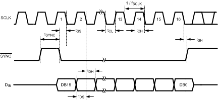 Figure 1. Serial Timing Diagram
7.7 Typical Characteristics
VA = 2.7 V to 5.5 V, VREF1,2 = VA, fSCLK = 30 MHz, TA = 25°C, unless otherwise stated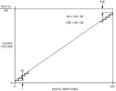 Figure 2. I/O Transfer Characteristic
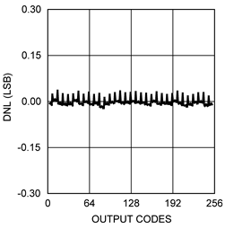 Figure 4. DNL vs Code
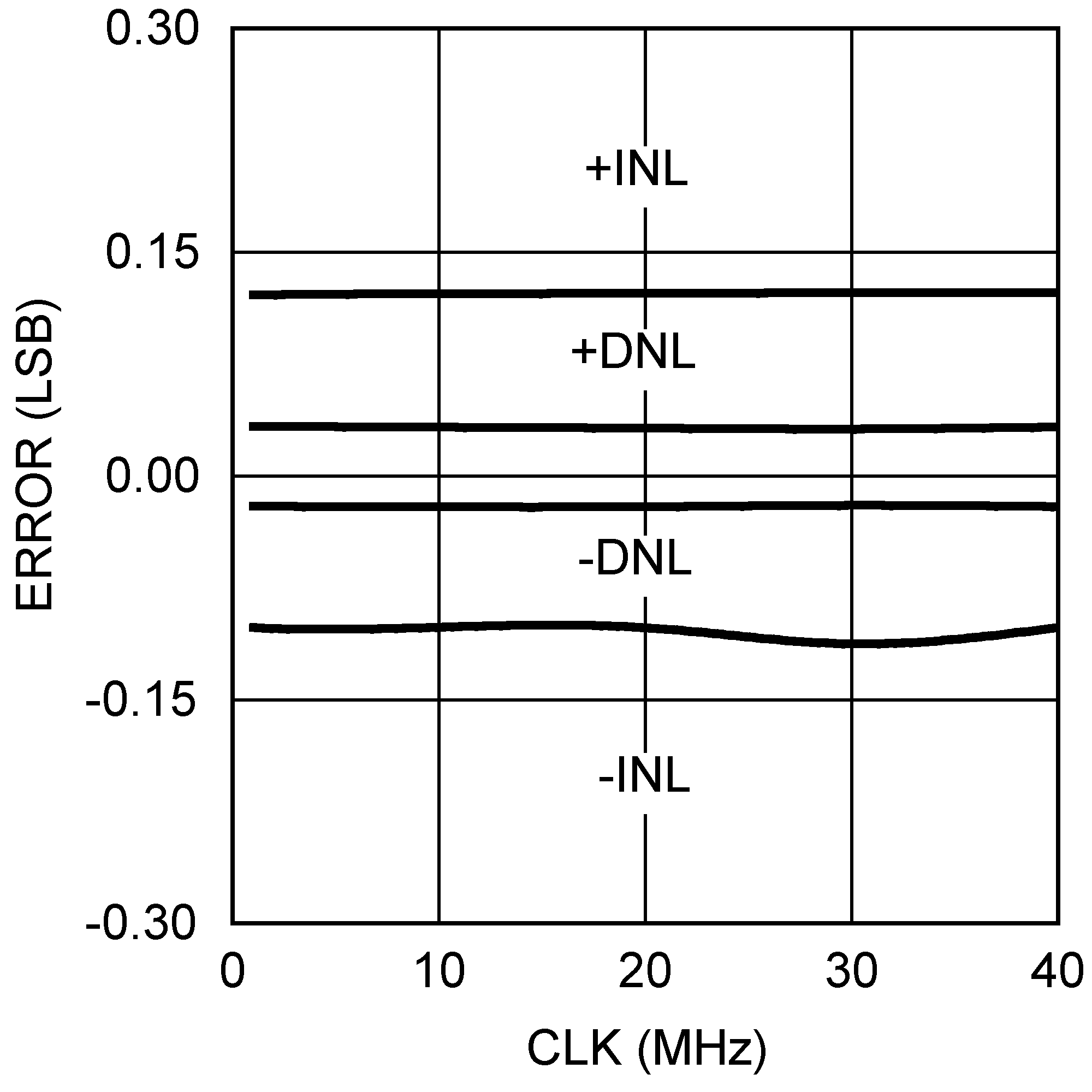 Figure 6. INL and DNL vs fSCLK
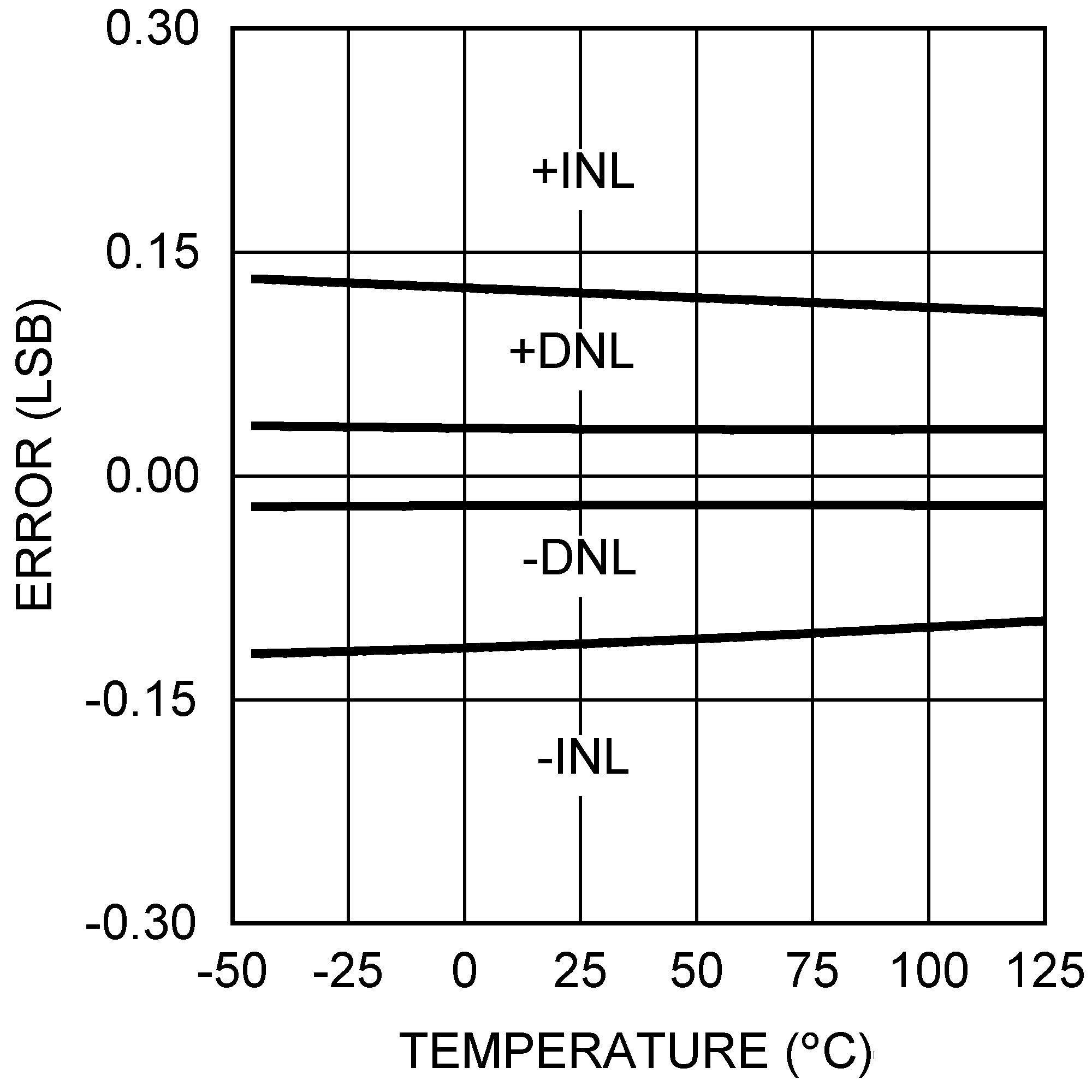 Figure 8. INL and DNL vs Temperature
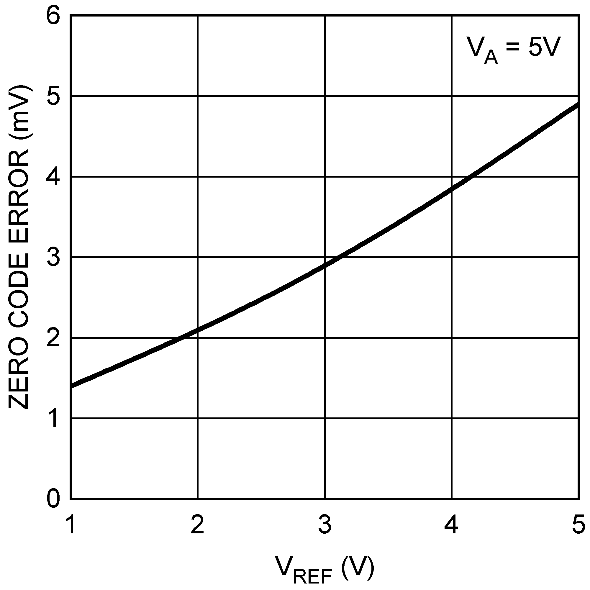 Figure 10. Zero Code Error vs VREF
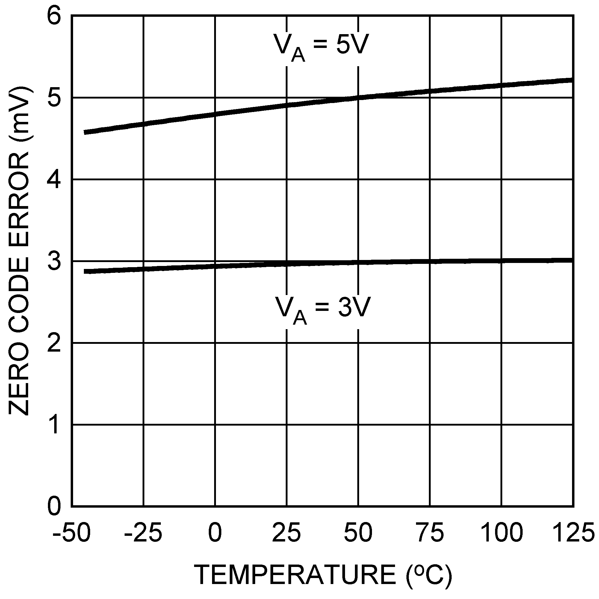 Figure 12. Zero Code Error vs Temperature
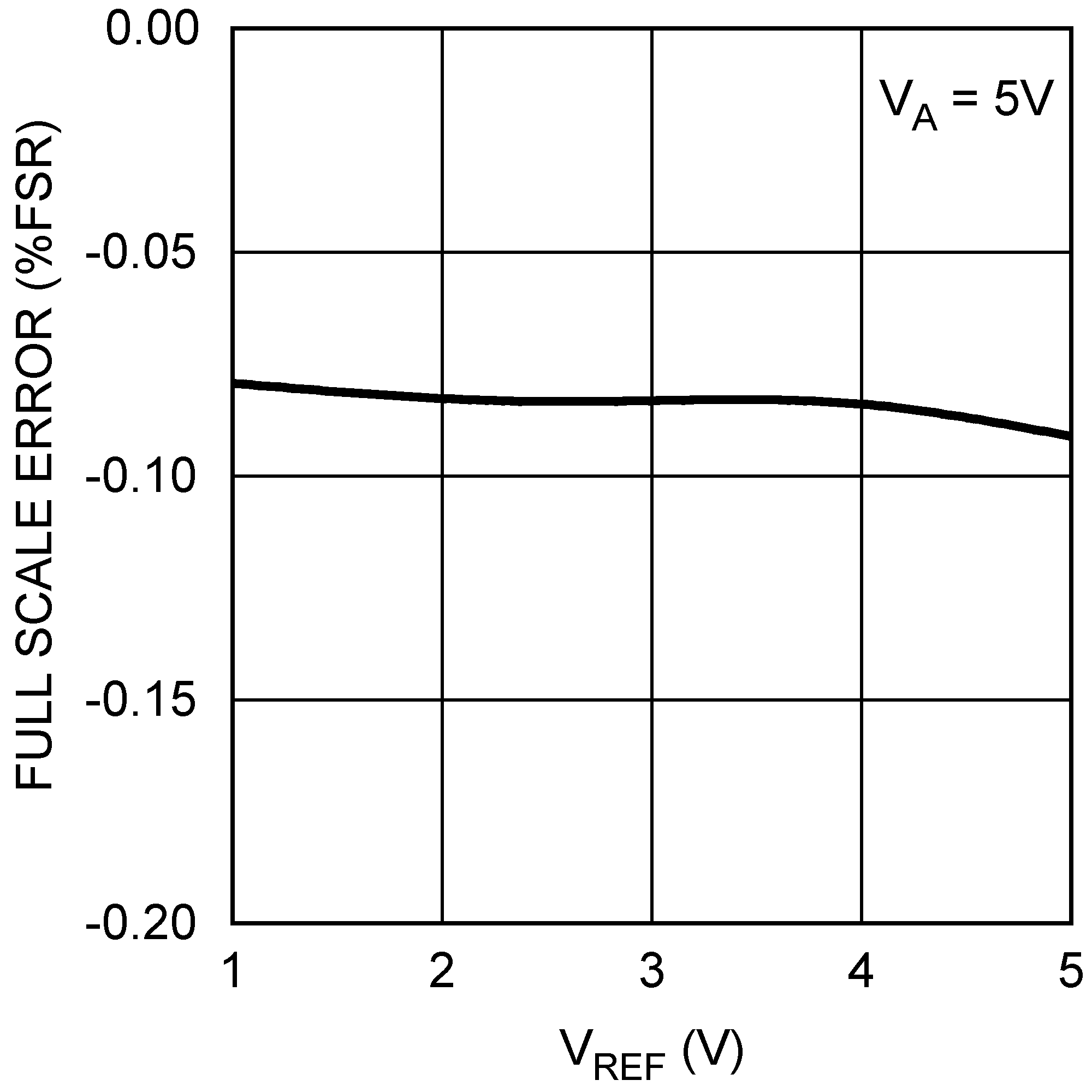 Figure 14. Full-Scale Error vs VREF
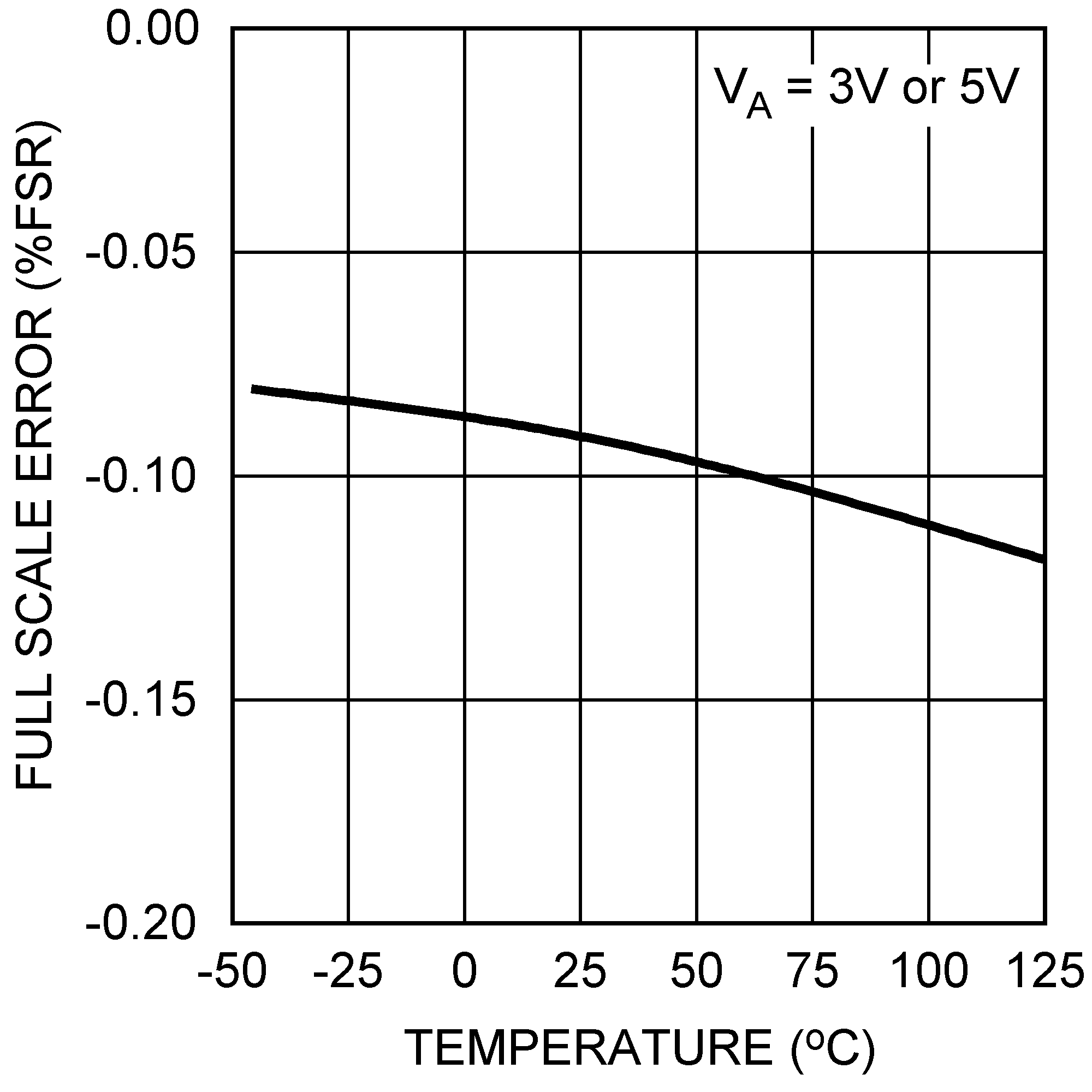 Figure 16. Full-Scale Error vs Temperature
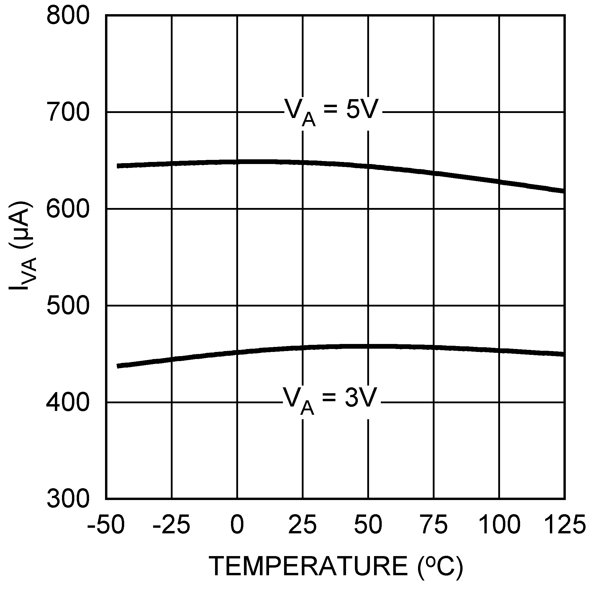 Figure 18. IVA vs Temperature
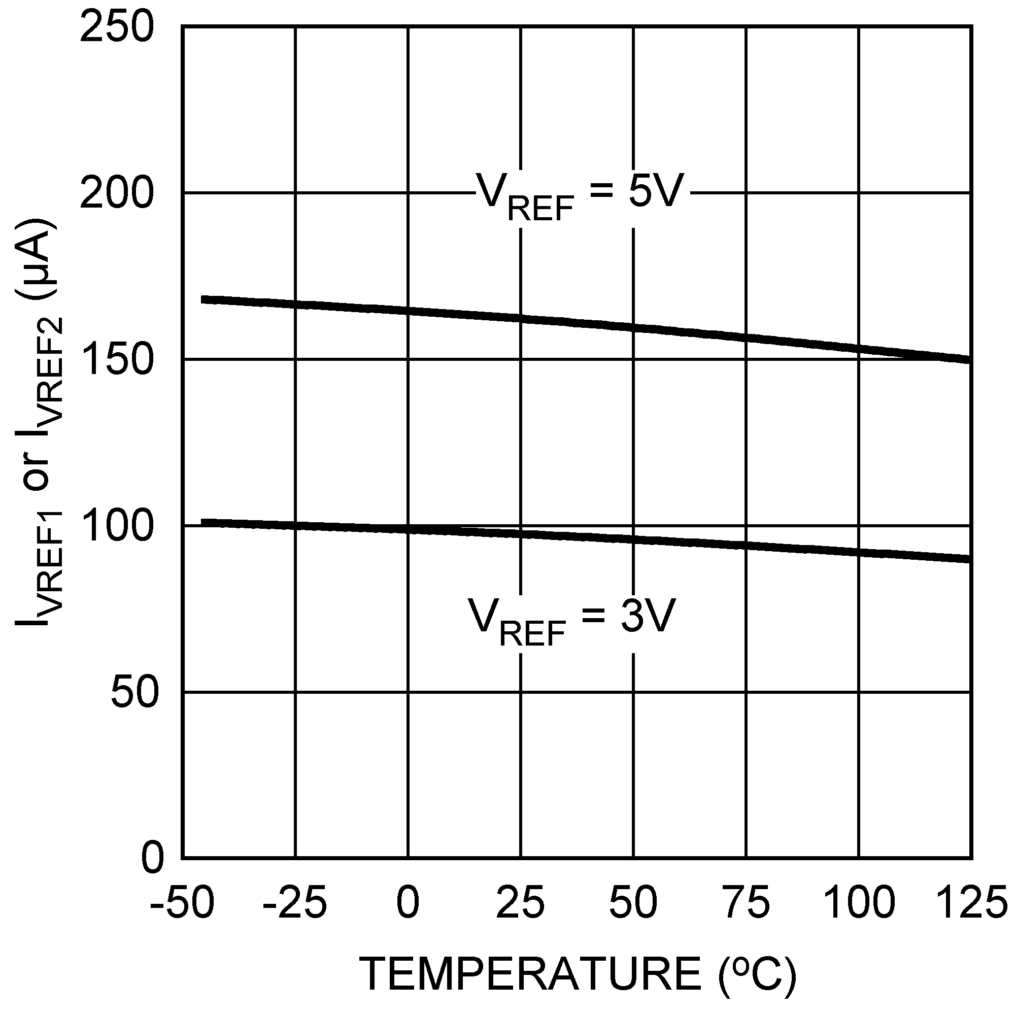 Figure 20. IVREF vs Temperature
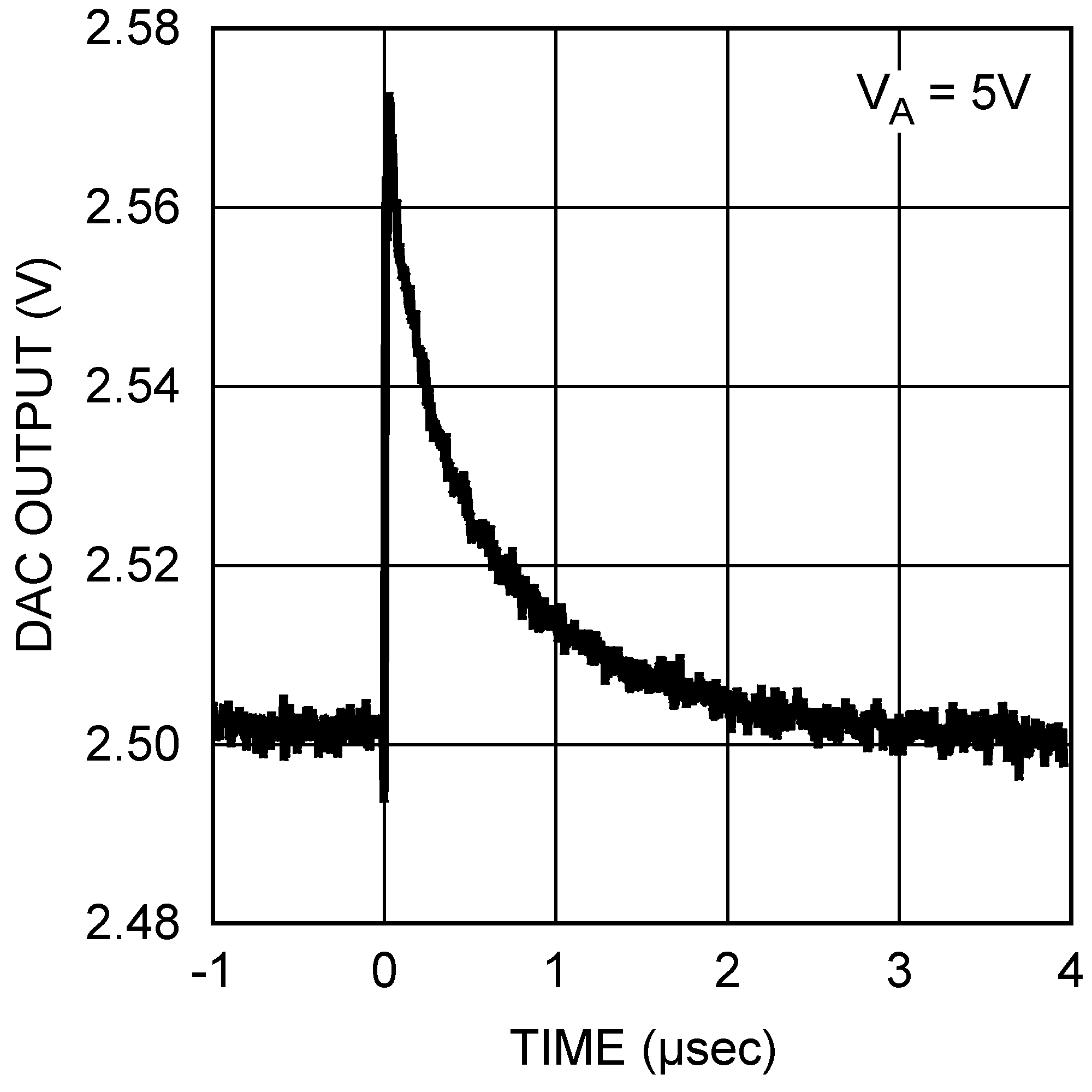 Figure 22. Glitch Response
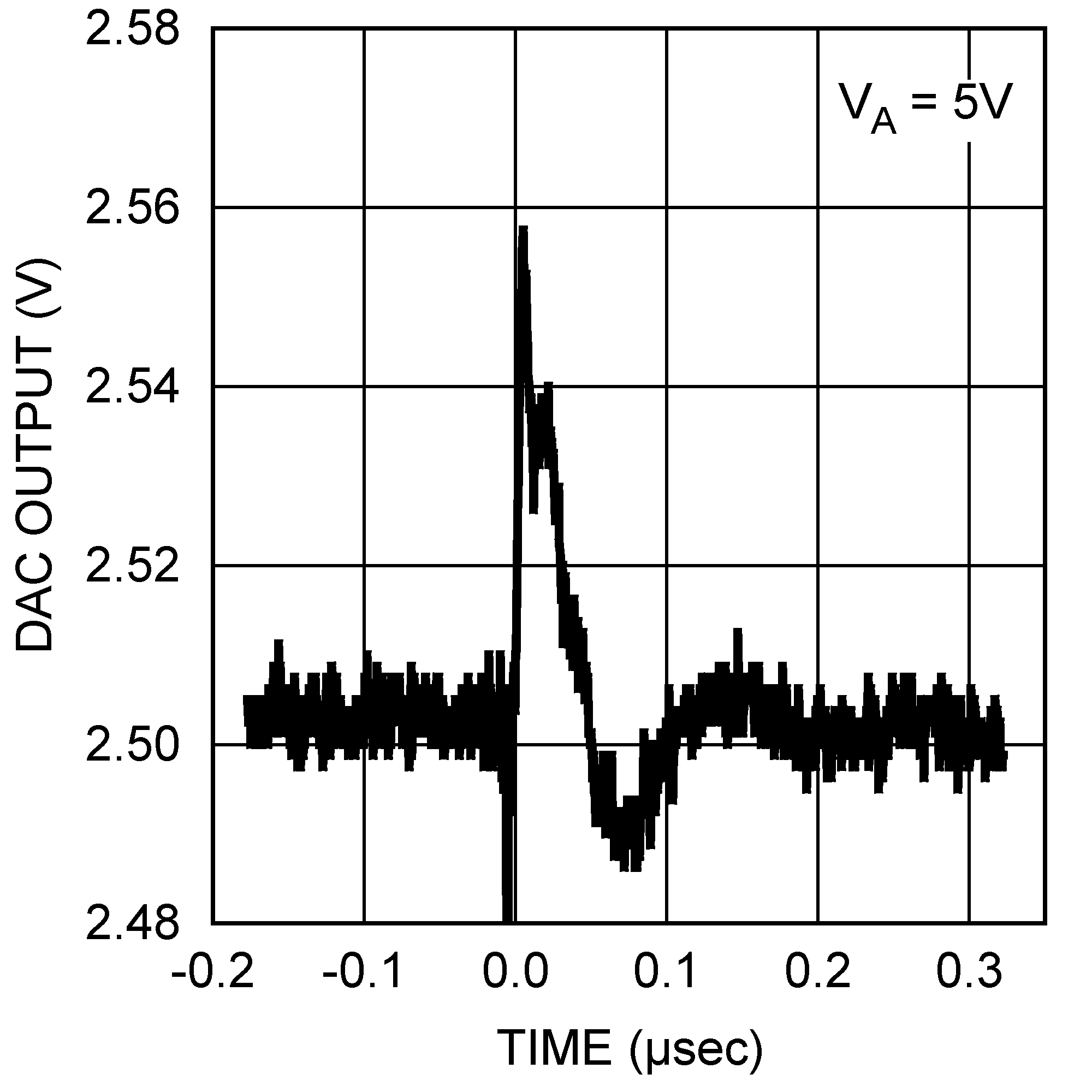 Figure 24. DAC-to-DAC Crosstalk
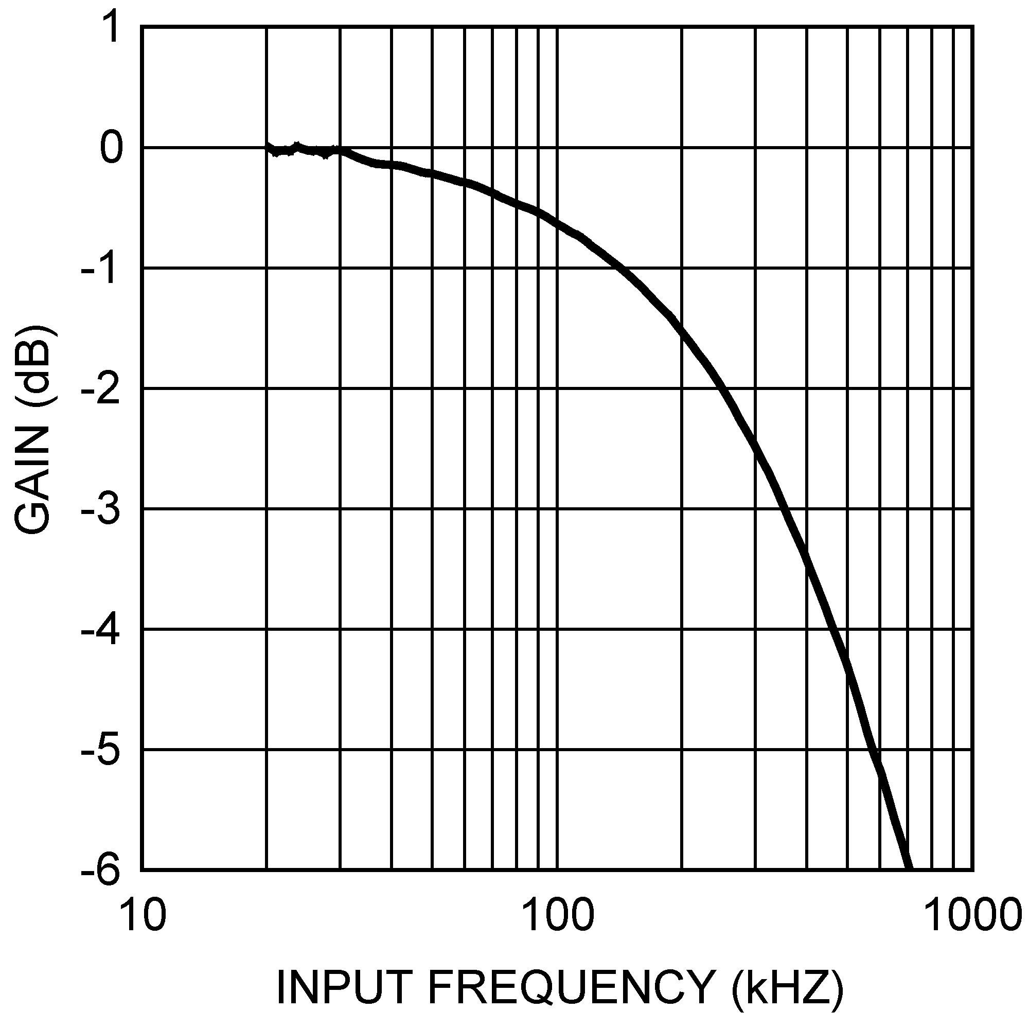 Figure 26. Multiplying Bandwidth
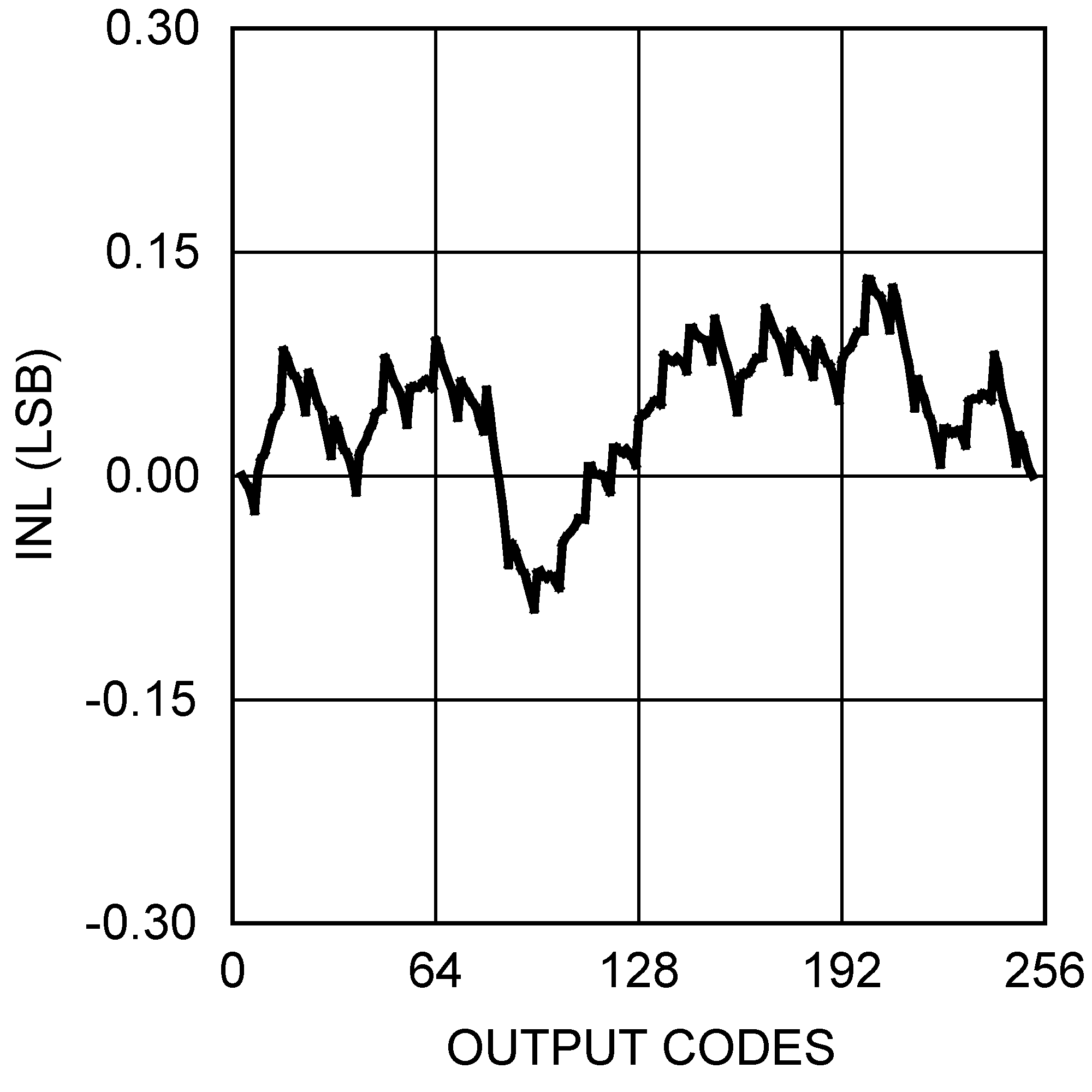 Figure 3. INL vs Code
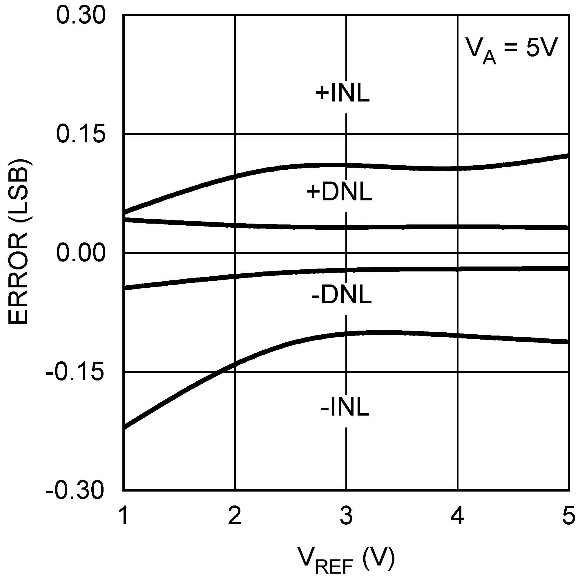 Figure 5. INL and DNL vs VREF
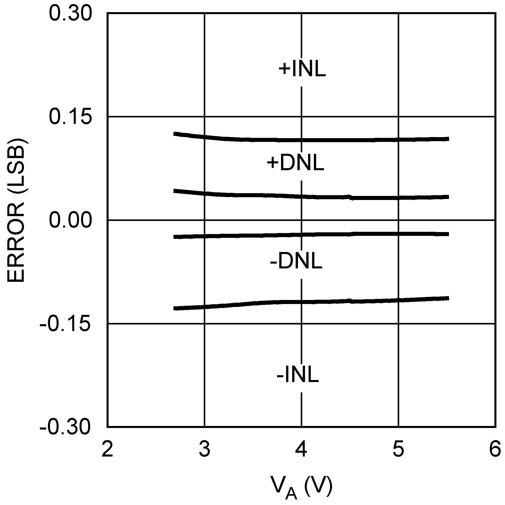 Figure 7. INL and DNL vs VA
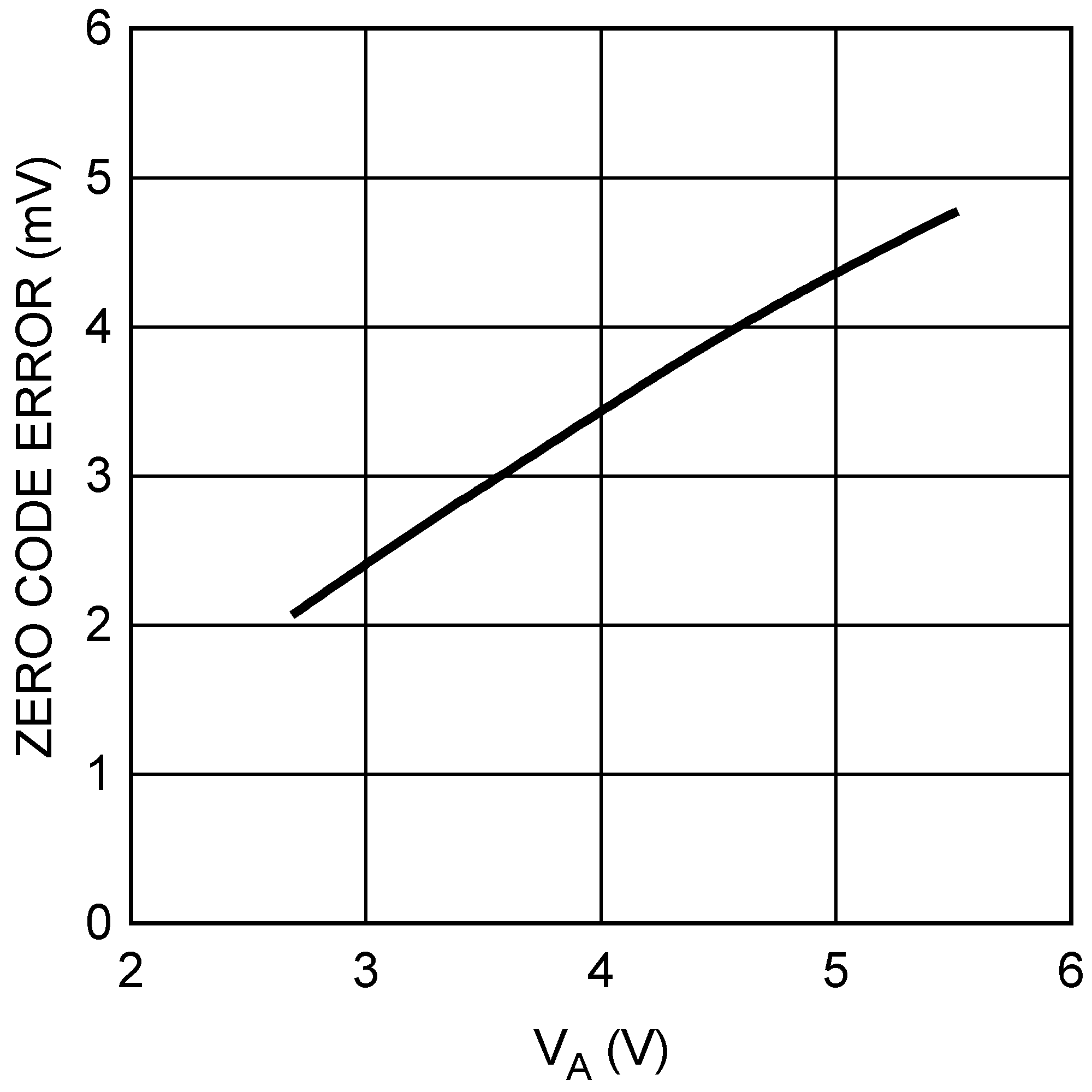 Figure 9. Zero Code Error vs VA
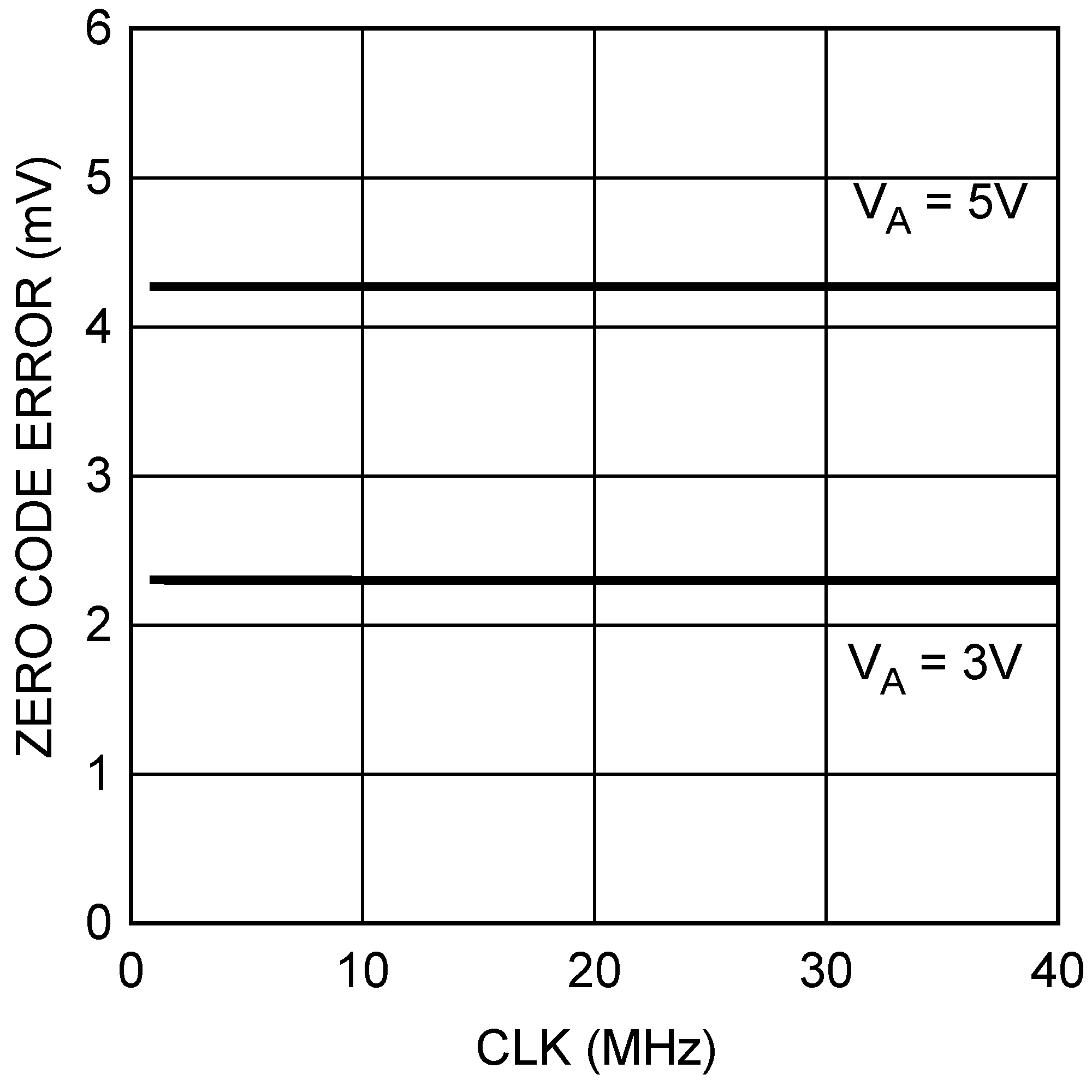 Figure 11. Zero Code Error vs fSCLK
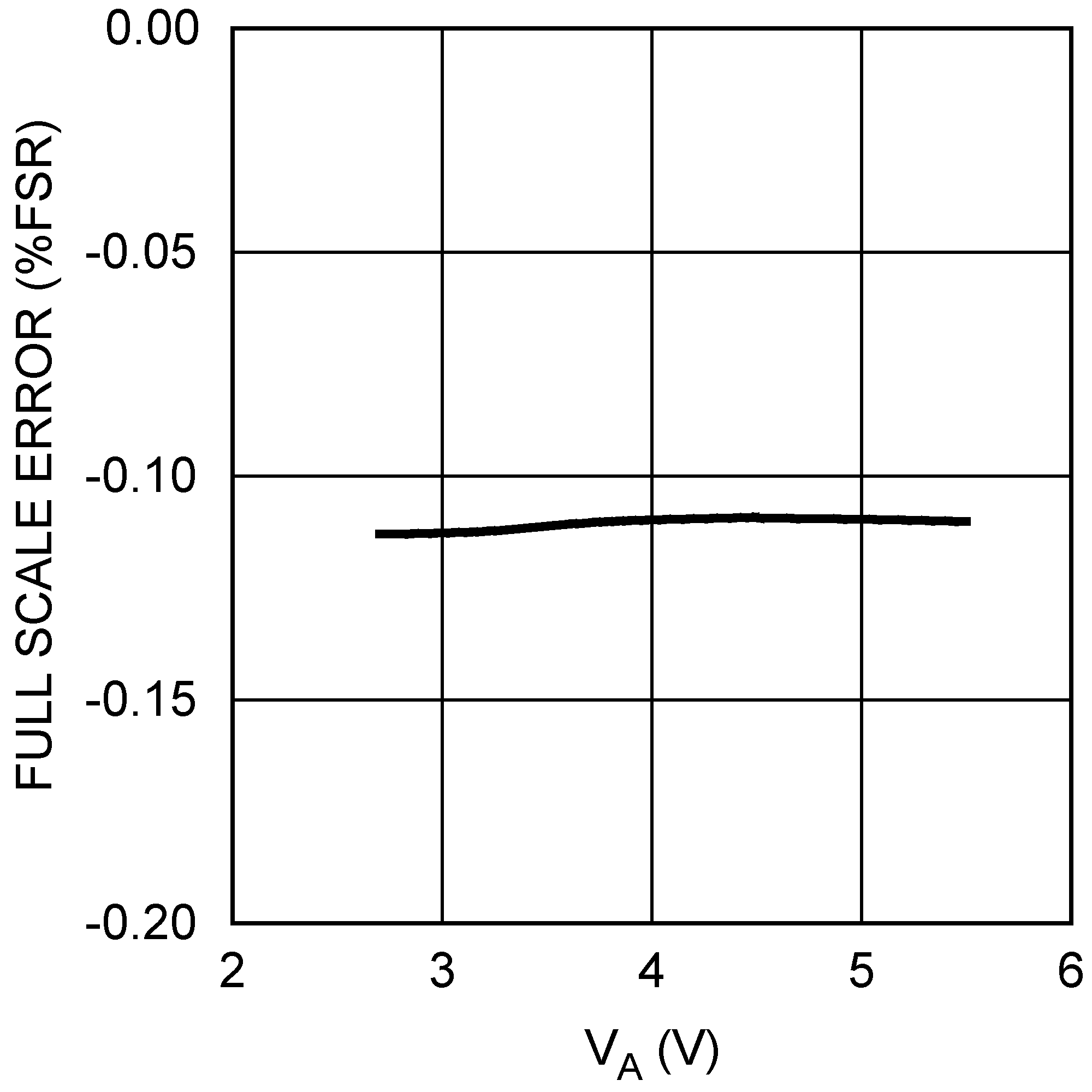 Figure 13. Full-Scale Error vs VA
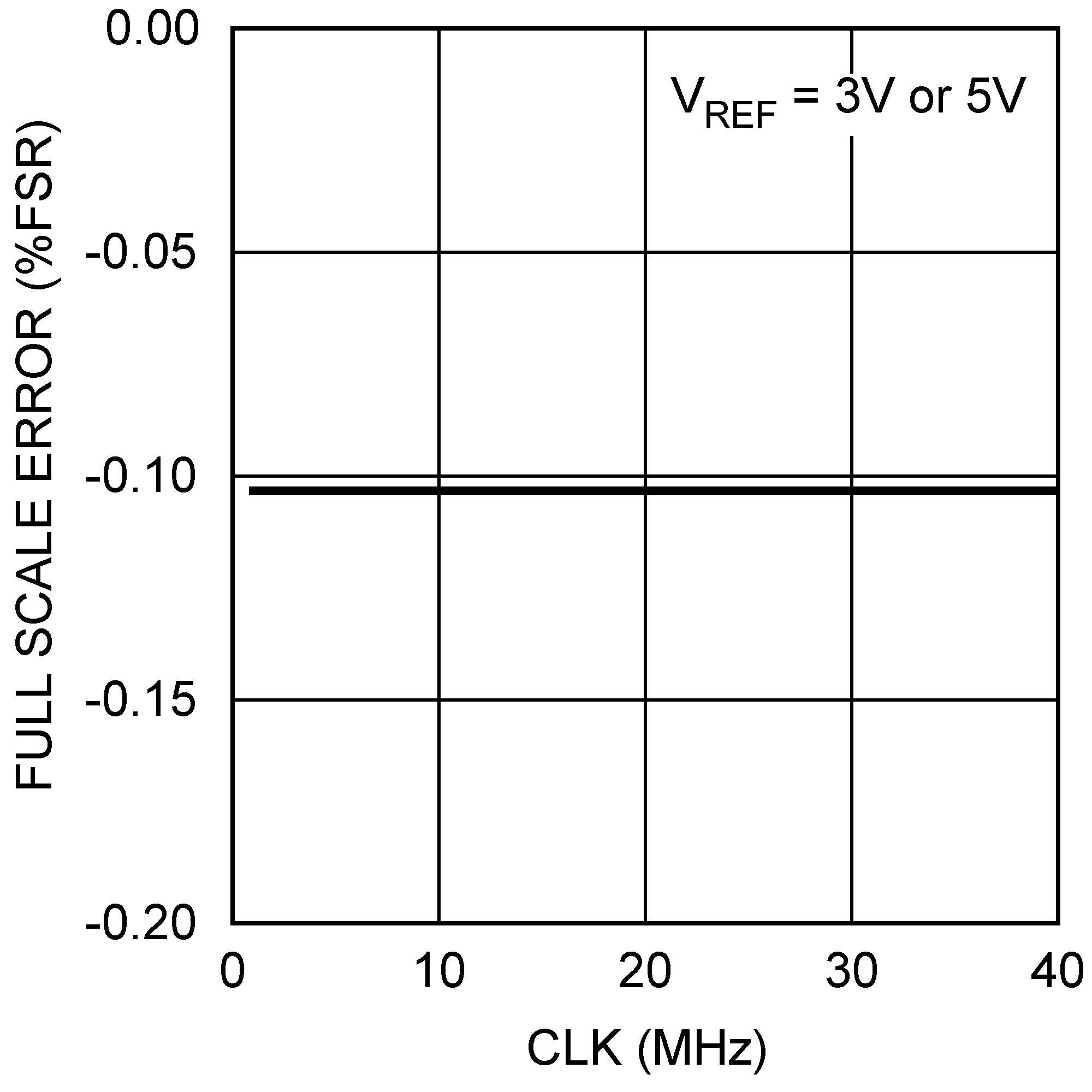 Figure 15. Full-Scale Error vs fSCLK
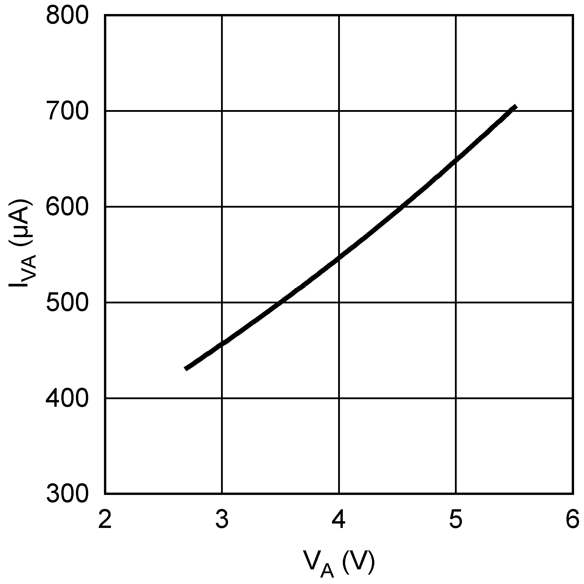 Figure 17. IVA vs VA
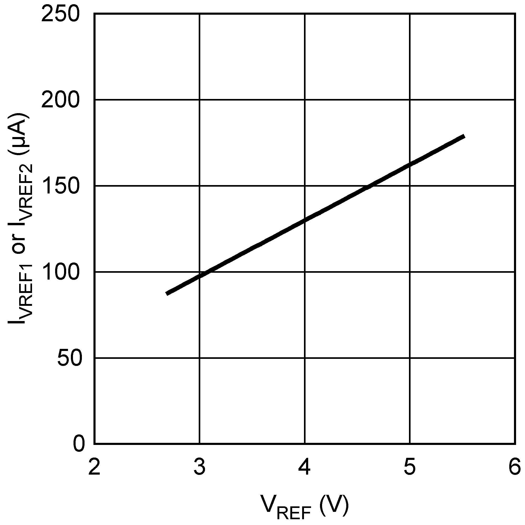 Figure 19. IVREF vs VREF
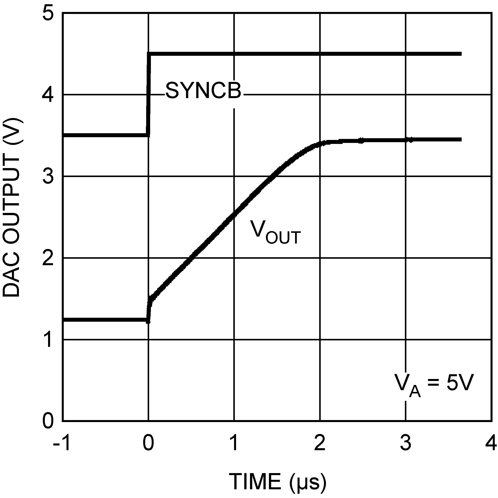 Figure 21. Settling Time
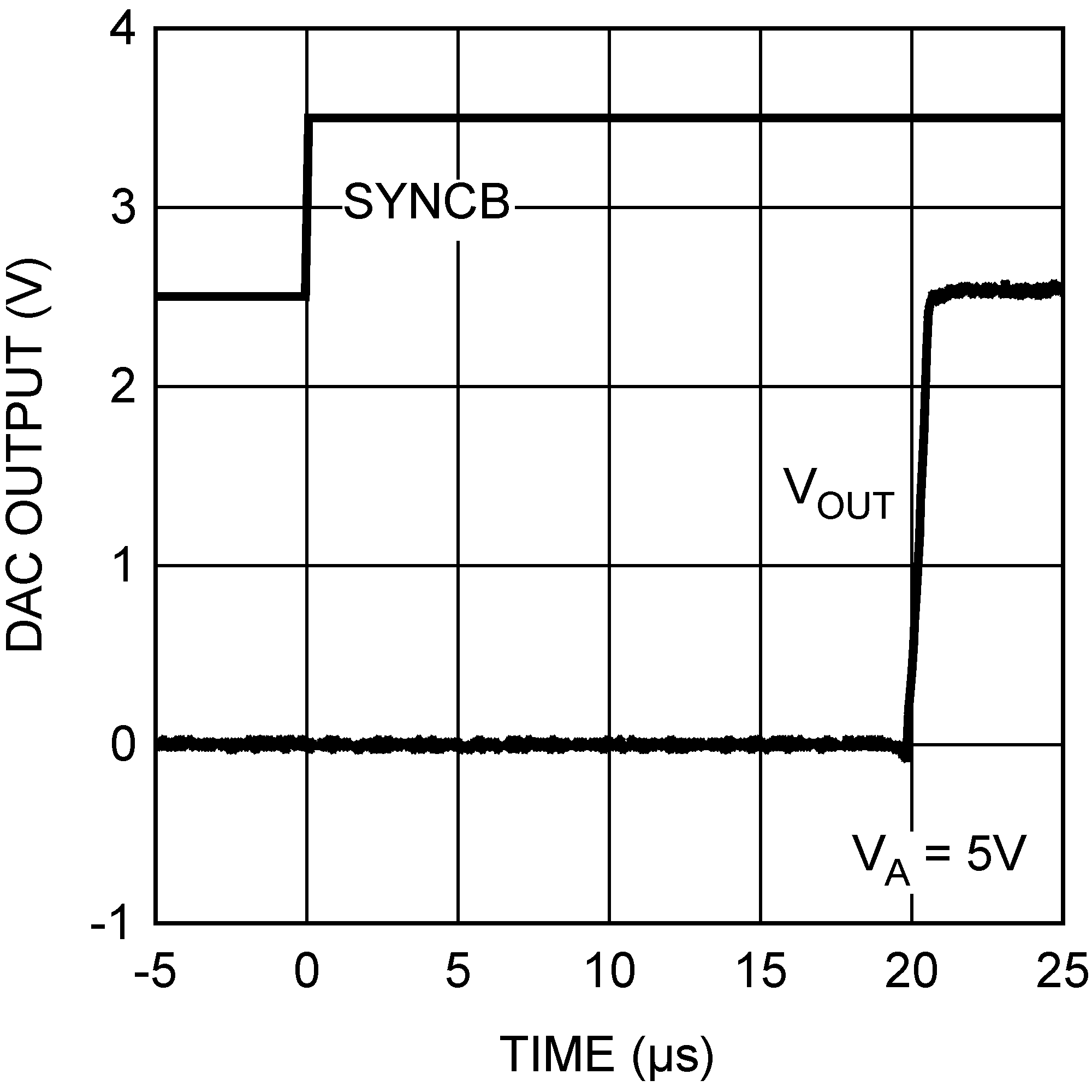 Figure 23. Wake-Up Time
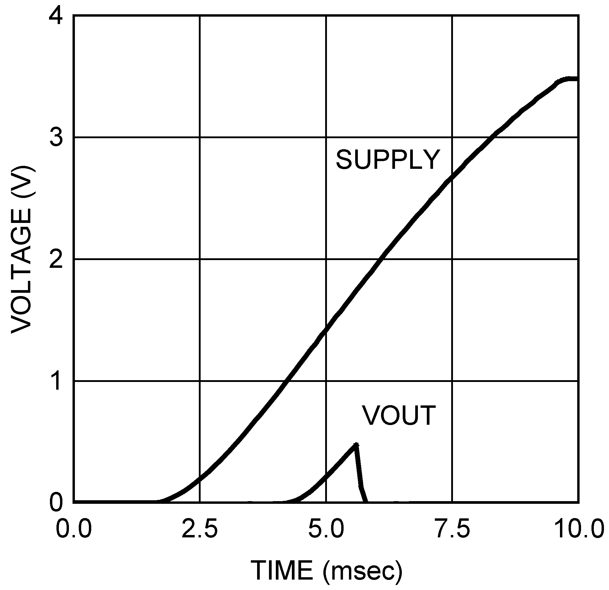 Figure 25. Power-On Reset