SNAS321G June 2005 – April 2016 DAC101S101 , DAC101S101-Q1
PRODUCTION DATA.
- 1 Features
- 2 Applications
- 3 Description
- 4 Revision History
- 5 Description (continued)
- 6 Pin Configuration and Functions
- 7 Specifications
- 8 Detailed Description
- 9 Application and Implementation
- 10Power Supply Recommendations
- 11Layout
- 12Device and Documentation Support
- 13Mechanical, Packaging, and Orderable Information
9 Application and Implementation
NOTE
Information in the following applications sections is not part of the TI component specification, and TI does not warrant its accuracy or completeness. TI’s customers are responsible for determining suitability of components for their purposes. Customers should validate and test their design implementation to confirm system functionality.
9.1 Application Information
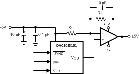
The DAC101S101 is designed for single supply operation and thus has a unipolar output. However, a bipolar output may be obtained with the circuit in Figure 41. This circuit will provide an output voltage range of ±5 Volts. A rail-to-rail amplifier should be used if the amplifier supplies are limited to ±5V.
9.2 Typical Application
 Figure 41. Bipolar Operation
9.2.1 Design Requirements
- The DAC101S101 will use a single supply.
- The output is required to be bipolar with a voltage range of ±5 V.
- Dual supplies will be used for the output amplifier.
9.2.2 Detailed Design Procedure
The output voltage of this circuit for any code is found to be
where
- D is the input code in decimal form
- With VA = 5V and R1 = R2
A list of rail-to-rail amplifiers suitable for this application are indicated in Table 2.
Table 2. Some Rail-To-Rail Amplifiers
| AMP | PKGS | Typ VOS | Typ ISUPPLY |
|---|---|---|---|
| LMC7111 | SOT-23-5 | 0.9 mV | 25 µA |
| LM7301 | SOIC-8 SOT-23-5 |
0.03 mV | 620 µA |
| LM8261 | SOT-23-5 | 0.7 mV | 1 mA |
9.2.3 Application Curve
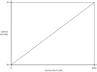
 Figure 42. Bipolar Input / Output Transfer Characteristic