ZHCSKD4A October   2019  – December 2019 DAC11001A , DAC81001 , DAC91001

UNLESS OTHERWISE NOTED, this document contains PRODUCTION DATA.  

  1. 特性
  2. 应用
  3. 说明
    1.     Device Images
      1.      功能方框图
      2.      高精度控制环路电路
  4. 修订历史记录
  5. Device Comparison Table
  6. Pin Configuration and Functions
    1.     Pin Functions
  7. Specifications
    1. 7.1      Absolute Maximum Ratings
    2. 7.2      ESD Ratings
    3. 7.3      Recommended Operating Conditions
    4. 7.4      Thermal Information Package
    5. 7.5      Electrical Characteristics
    6. Table 1. Timing Requirements: Write, 4.5 V ≤ DVDD ≤ 5.5 V
    7. Table 2. Timing Requirements: Write, 2.7 V ≤ DVDD < 4.5 V
    8. Table 3. Timing Requirements: Read and Daisy-Chain Write, 4.5 V ≤ DVDD ≤ 5.5 V
    9. Table 4. Timing Requirements: Read and Daisy-Chain Write, 2.7 V ≤ DVDD < 4.5 V
    10. 7.6      Typical Characteristics
  8. Detailed Description
    1. 8.1 Overview
    2. 8.2 Functional Block Diagram
    3. 8.3 Feature Description
      1. 8.3.1 Digital-to-Analog Converter Architecture
      2. 8.3.2 External Reference
      3. 8.3.3 Output Buffers
      4. 8.3.4 Internal Power-On Reset (POR)
      5. 8.3.5 Temperature Drift and Calibration
      6. 8.3.6 DAC Output Deglitch Circuit
    4. 8.4 Device Functional Modes
      1. 8.4.1 Fast-Settling Mode and THD
      2. 8.4.2 DAC Update Rate Mode
    5. 8.5 Programming
      1. 8.5.1 Daisy-Chain Operation
      2. 8.5.2 CLR Pin Functionality and Software Clear
      3. 8.5.3 Output Update (Synchronous and Asynchronous)
        1. 8.5.3.1 Synchronous Update
        2. 8.5.3.2 Asynchronous Update
      4. 8.5.4 Software Reset Mode
    6. 8.6 Register Map
      1. 8.6.1 NOP Register (address = 00h) [reset = 0x000000h]
        1. Table 9. NOP Register Field Descriptions
      2. 8.6.2 DAC-DATA Register (address = 01h) [reset = 0x000000h]
        1. Table 10. DAC-DATA Register Field Descriptions
      3. 8.6.3 CONFIG1 Register (address = 02h) [reset = 004C80h for bits [23:0]]
        1. Table 11. CONFIG1 Register Field Descriptions
      4. 8.6.4 DAC-CLEAR-DATA Register (address = 03h) [reset = 000000h for bits [23:0]]
        1. Table 12. DAC-CLEAR-DATA Register Field Descriptions
      5. 8.6.5 TRIGGER Register (address = 04h) [reset = 000000h for bits [23:0]]
        1. Table 13. TRIGGER Register Field Descriptions
      6. 8.6.6 STATUS Register (address = 05h) [reset = 000000h for bits [23:0]]
        1. Table 14. STATUS Register Field Descriptions
      7. 8.6.7 CONFIG2 Register (address = 06h) [reset = 000040h for bits [23:0]]
        1. Table 15. CONFIG2 Register Field Descriptions
  9. Application and Implementation
    1. 9.1 Application Information
    2. 9.2 Typical Application
      1. 9.2.1 Source Measure Unit (SMU)
        1. 9.2.1.1 Design Requirements
        2. 9.2.1.2 Detailed Design Procedure
        3. 9.2.1.3 Application Curves
      2. 9.2.2 Battery Test Equipment (BTE)
        1. 9.2.2.1 Design Requirements
        2. 9.2.2.2 Detailed Design Procedure
        3. 9.2.2.3 Application Curves
      3. 9.2.3 High-Precision Control Loop
        1. 9.2.3.1 Design Requirements
        2. 9.2.3.2 Detailed Design Procedure
        3. 9.2.3.3 Application Curves
      4. 9.2.4 Arbitrary Waveform Generation (AWG)
        1. 9.2.4.1 Design Requirements
        2. 9.2.4.2 Detailed Design Procedure
        3. 9.2.4.3 Application Curves
    3. 9.3 System Examples
      1. 9.3.1 Interfacing to a Processor
      2. 9.3.2 Interfacing to a Low-Jitter LDAC Source
      3. 9.3.3 Embedded Resistor Configurations
        1. 9.3.3.1 Minimizing Bias Current Mismatch
        2. 9.3.3.2 2x Gain configuration
        3. 9.3.3.3 Generating Negative Reference
    4. 9.4 What to Do and What Not to Do
      1. 9.4.1 What to Do
      2. 9.4.2 What Not to Do
    5. 9.5 Initialization Set Up
  10. 10Power Supply Recommendations
    1. 10.1 Power-Supply Sequencing
  11. 11Layout
    1. 11.1 Layout Guidelines
    2. 11.2 Layout Example
  12. 12器件和文档支持
    1. 12.1 器件支持
      1. 12.1.1 开发支持
    2. 12.2 文档支持
      1. 12.2.1 相关文档
    3. 12.3 相关链接
    4. 12.4 接收文档更新通知
    5. 12.5 支持资源
    6. 12.6 商标
    7. 12.7 静电放电警告
    8. 12.8 Glossary
  13. 13机械、封装和可订购信息

封装选项

机械数据 (封装 | 引脚)
散热焊盘机械数据 (封装 | 引脚)
订购信息

Minimizing Bias Current Mismatch

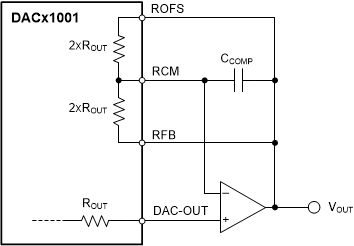
The bias current mismatch in the output amplifier can lead to offset error at the output. To minimize mismatch, the amplifier must have a matching resistor to that of the R2R output impedance on the feedback path. The feedback resistors are used in parallel for this purpose, as shown in Figure 69. Some amplifiers may become unstable with a feedback resistor in the buffer configuration. Therefore, a compensation capacitor (CCOMP) might be needed, as shown. The typical value of this capacitor is in the range of 22 pF to 100 pF, depending on the amplifier.
DAC11001A DAC91001 DAC81001 dac11001-bias-current-compensation.gifFigure 69. Minimizing Bias Current Mismatch