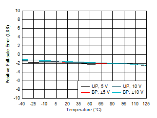
at TA = 25°C,
VCC = 15 V, VSS = –15 V, AVDD = 5 V, IOVDD =
1.8 V, gain resistors unconnected (gain = 1x), OPA827 used as reference amplifier, OPA828
used as output amplifier, UP = unipolar, BP = bipolar, and temperature calibration disabled (unless otherwise noted)
Figure 6-3 Integral Linearity Error vs Digital
Input CodeFigure 6-5 Integral Linearity Error vs
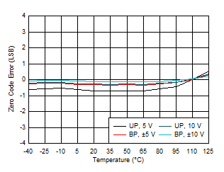
TemperatureFigure 6-7 Zero Code Error vs
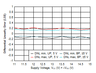
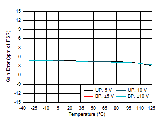
TemperatureFigure 6-9 Gain Error vs TemperatureFigure 6-11 Differential Linearity Error vs
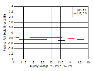
Supply VoltageFigure 6-13 Positive Full-Scale Error vs Supply
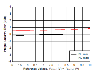
VoltageFigure 6-15 Integral Linearity Error vs
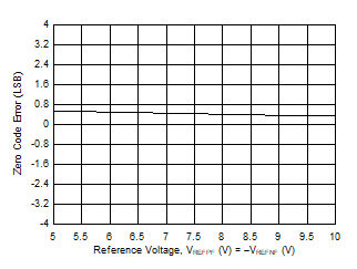
Reference VoltageFigure 6-17 Zero Code Error
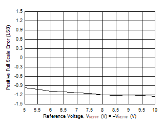
vs Reference VoltageFigure 6-19 Positive Full-Scale Error vs
Reference Voltage
VREFPF = 10 V,
VREFNF = 0 V
Figure 6-21 Supply Current (VCC and
VSS )
VREFPF = 10 V,
VREFNF = 0 V
Figure 6-23 Supply Current (AVDD ) vs
Digital Input Code
VREFPF = 10 V,
VREFNF = 0 V, DAC at midcode
Figure 6-25 Supply Current (VCC and
VSS )
VREFPF = 10 V,
VREFNF = 0 V, DAC at midcode
Figure 6-27 Supply Current (AVDD ) vs
Temperature
VREFPF = 10 V,
VREFNF = 0 V, DAC at midcode
Figure 6-29 Supply Current (IOVDD )
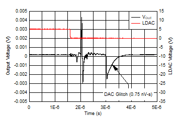
VREFPF = 10 V,
VREFNF = –10 V,
DAC transition midcode – 1
to midcode
Figure 6-31 Glitch Impulse, Rising Edge, 1-LSB
Step
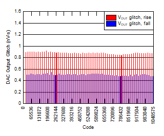
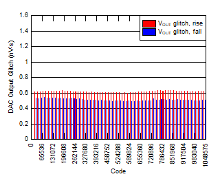
VREFPF = 10 V,
VREFNF = –10 V
Figure 6-33 Segment Glitch Impulse, 1-LSB
Step
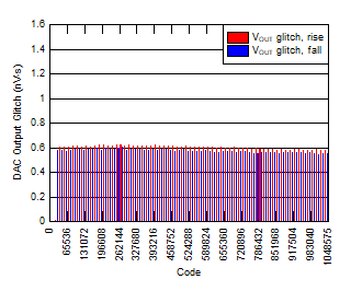
VREFPF = 5 V,
VREFNF = 0 V
Figure 6-35 Segment Glitch Impulse, 1-LSB
Step
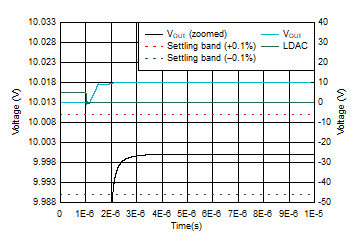
VREFPF = 10 V,
VREFNF = 0 V
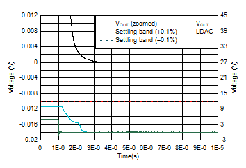
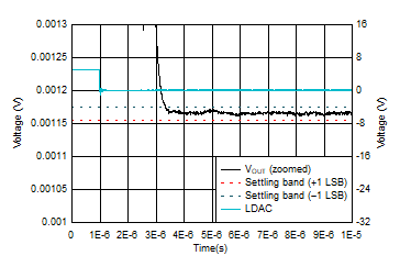
Figure 6-37 Full-Scale Settling Time, Rising
Edge
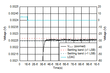
VREFPF = 10 V,
VREFNF = 0 V,
DAC transitions 100 codes
around midscale
Figure 6-39 100 Codes Settling Time, Rising
Edge
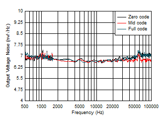
VREFPF = 10 V,
VREFNF = 0 V, measured at DAC output
Figure 6-41 DAC Output Noise Spectral
Density
DAC update rate = 768 kHz,
VREFPF = 4.5 V, VREFNF = −4.5 V, sixth-order,
low-pass, 30-kHz output filter
Figure 6-43 1-kHz Spectrum vs Frequency
DAC update rate = 1 MHz,
VREFPF = 4.5 V, VREFNF = −4.5 V, sixth-order,
low-pass, 150-kHz output filter
Figure 6-45 100-kHz Spectrum vs
Frequency
DAC update rate = 768 kHz,
VREFPF = 4.5 V, VREFNF = −4.5 V, sixth-order,
low-pass, 30-kHz output filter
Figure 6-47 Total Harmonic Distortion DAC = 768 kHz
DAC update rate = 768 kHz,
VREFPF = 4.5 V, VREFNF = −4.5 V, sixth-order,
low-pass, 30-kHz output filter
Figure 6-49 Second Harmonic Distortion DAC = 768 kHz
DAC update rate = 1 MHz,
VREFPF = 4.5 V, VREFNF = −4.5 V, sixth-order,
low-pass, 150-kHz output filter
Figure 6-51 Spurious Free Dynamic Range DAC = 1 MHz
DAC update rate = 1 MHz,
VREFPF = 4.5 V, VREFNF = −4.5 V, sixth-order,
low-pass, 150-kHz output filter
Figure 6-53 Total Harmonic Distortion + Noise
DAC = 1 MHz
DAC update rate = 1 MHz,
VREFPF = 4.5 V, VREFNF = −4.5 V, sixth-order,
low-pass, 150-kHz output filter
Figure 6-55 Third Harmonic Distortion DAC = 1 MHz
DAC output frequency = 20
kHz, VREFPF = 4.5 V, VREFNF = −4.5 V, sixth-order,
low-pass, 30-kHz output filter
Figure 6-57 Total Harmonic Distortion vs Update
Rate
DAC output frequency = 20
kHz, VREFPF = 4.5 V, VREFNF = −4.5 V, sixth-order,
low-pass, 30-kHz output filter
Figure 6-59 Second Harmonic Distortion vs Update
RateFigure 6-4 Differential Linearity Error vs
Digital Input CodeFigure 6-6 Differential Linearity Error vs
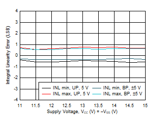
TemperatureFigure 6-8 Positive Full-Scale Error vs
TemperatureFigure 6-10 Integral Linearity Error vs Supply
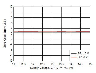
VoltageFigure 6-12 Zero Code Error vs Supply
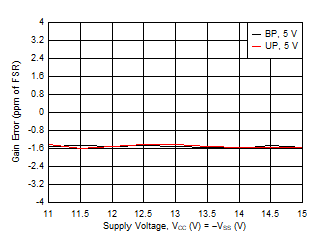
VoltageFigure 6-14 Gain Error vs Supply VoltageFigure 6-16 Differential
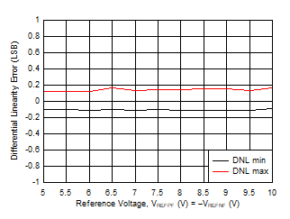
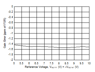
Linearity Error vs Reference VoltageFigure 6-18 Gain Error vs
Reference Voltage
VREFPF = 10 V,
VREFNF = 0 V
Figure 6-20 Supply Current (DVDD and
IOVDD ) vs Digital Input Code
VREFPF = 10 V,
VREFNF = 0 V
Figure 6-22 Reference Current (VREFPF
and VREFNF ) vs Digital Input Code
VREFPF = 10 V,
VREFNF = 0 V, DAC at midcode
Figure 6-24 Supply Current (DVDD ) vs
Temperature
VREFPF = 10 V,
VREFNF = 0 V, DAC at midcode
Figure 6-26 Reference Current (VREFPF
and VREFNF )
VREFPF = 5 V,
VREFNF = 0 V, DAC at midcode
Figure 6-28 Supply Current (VCC and
VSS ) vs Supply Voltage
VREFPF = 10 V,
VREFNF = 0 V, DAC at midcode
Figure 6-30 Supply Current (IOVDD )
VREFPF = 10 V,
VREFNF = –10 V,
DAC transition midcode to
midcode – 1
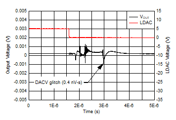
Figure 6-32 Glitch Impulse, Falling Edge, 1-LSB
Step
VREFPF = 10 V,
VREFNF = 0 V
Figure 6-34 Segment Glitch Impulse, 1-LSB
Step
VREFPF = 10 V,
VREFNF = 0 V,
DAC at midcode, measured
at DAC output pin
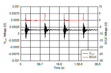
Figure 6-36 Clock Feedthrough
VREFPF = 10 V,
VREFNF = 0 V
Figure 6-38 Full-Scale Settling Time, Falling
Edge
VREFPF = 10 V,
VREFNF = 0 V,
DAC transitions 100 codes
around midscale
Figure 6-40 100 Codes Settling Time, Falling
Edge
VREFPF = 10 V,
VREFNF = 0 V,
DAC at midcode, measured
at DAC output pin
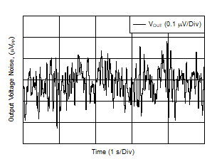
Figure 6-42 DAC Output Noise: 0.1 Hz to 10
Hz
DAC update rate = 768 kHz,
VREFPF = 4.5 V, VREFNF = −4.5 V, sixth-order,
low-pass, 30-kHz output filter
Figure 6-44 20-kHz Spectrum vs Frequency
DAC update rate = 768 kHz,
VREFPF = 4.5 V, VREFNF = −4.5 V, sixth-order,
low-pass, 30-kHz output filter
Figure 6-46 Spurious Free Dynamic Range DAC = 768 kHz
DAC update rate = 768 kHz,
VREFPF = 4.5 V, VREFNF = −4.5 V, sixth-order,
low-pass, 30-kHz output filter
Figure 6-48 Total Harmonic Distortion + Noise
DAC = 768 kHz
DAC update rate = 768 kHz,
VREFPF = 4.5 V, VREFNF = −4.5 V, sixth-order,
low-pass, 30-kHz output filter
Figure 6-50 Third Harmonic Distortion DAC = 768 kHz
DAC update rate = 1 MHz,
VREFPF = 4.5 V, VREFNF = −4.5 V, sixth-order,
low-pass, 150-kHz output filter
Figure 6-52 Total Harmonic Distortion DAC = 1 MHz
DAC update rate = 1 MHz,
VREFPF = 4.5 V, VREFNF = −4.5 V, sixth-order,
low-pass, 150-kHz output filter
Figure 6-54 Second Harmonic Distortion DAC = 1 MHz
DAC output frequency = 20
kHz, VREFPF = 4.5 V, VREFNF = −4.5 V, sixth-order,
low-pass, 30-kHz output filter
Figure 6-56 Spurious Free Dynamic Range vs
Update Rate
DAC output frequency = 20
kHz, VREFPF = 4.5 V, VREFNF = −4.5 V, sixth-order,
low-pass, 30-kHz output filter
Figure 6-58 Total Harmonic Distortion + Noise vs
Update Rate
DAC output frequency = 20
kHz, VREFPF = 4.5 V, VREFNF = −4.5 V, sixth-order,
low-pass, 30-kHz output filter
Figure 6-60 Third Harmonic Distortion vs Update
Rate
