SNAS265J June 2005 – September 2015 DAC121S101 , DAC121S101-Q1
PRODUCTION DATA.
- 1 Features
- 2 Applications
- 3 Description
- 4 Revision History
- 5 Description continued
- 6 Pin Configuration and Functions
- 7 Specifications
- 8 Detailed Description
- 9 Application and Implementation
- 10Power Supply Recommendations
- 11Layout
- 12Device and Documentation Support
- 13Mechanical, Packaging, and Orderable Information
9 Application and Implementation
NOTE
Information in the following applications sections is not part of the TI component specification, and TI does not warrant its accuracy or completeness. TI’s customers are responsible for determining suitability of components for their purposes. Customers should validate and test their design implementation to confirm system functionality.
9.1 Application Information
9.1.1 DSP and Microprocessor Interfacing
The simplicity of the DAC121S101 implies ease of use. However, it is important to recognize that any data converter that uses its supply voltage as its reference voltage will have essentially zero PSRR (power supply rejection ratio). Therefore, it is necessary to provide a noise-free supply voltage to the device.
Interfacing the DAC121S101 to microprocessors and DSPs is quite simple. The following guidelines are offered to hasten the design process.
9.1.1.1 ADSP-2101/ADSP2103 Interfacing
Figure 35 shows a serial interface between the DAC121S101 and the ADSP-2101/ADSP2103. The DSP must be set to operate in the SPORT Transmit Alternate Framing Mode. It is programmed through the SPORT control register and must be configured for Internal Clock Operation, Active Low Framing and 16-bit Word Length. Transmission is started by writing a word to the Tx register after the SPORT mode has been enabled.
 Figure 35. ADSP-2101/2103 Interface
9.1.1.1.1 80C51/80L51 Interface
A serial interface between the DAC121S101 and the 80C51/80L51 microcontroller is shown in Figure 36. The SYNC signal comes from a bit-programmable pin on the microcontroller. The example shown here uses port line P3.3. This line is taken low when data is to transmitted to the DAC121S101. Because the 80C51/80L51 transmits 8-bit bytes, only eight falling clock edges occur in the transmit cycle. To load data into the DAC, the P3.3 line must be left low after the first eight bits are transmitted. A second write cycle is initiated to transmit the second byte of data, after which port line P3.3 is brought high. The 80C51/80L51 transmit routine must recognize that the 80C51/80L51 transmits data with the LSB first while the DAC121S101 requires data with the MSB first.
 Figure 36. 80C51/80L51 Interface
9.1.1.1.2 68HC11 Interface
A serial interface between the DAC121S101 and the 68HC11 microcontroller is shown in Figure 37. The SYNC line of the DAC121S101 is driven from a port line (PC7 in the figure), similar to the 80C51/80L51.
The 68HC11 must be configured with its CPOL bit as a zero and its CPHA bit as a one. This configuration causes data on the MOSI output to be valid on the falling edge of SCLK. PC7 is taken low to transmit data to the DAC. The 68HC11 transmits data in 8-bit bytes with eight falling clock edges. Data is transmitted with the MSB first. PC7 must remain low after the first eight bits are transferred. A second write cycle is initiated to transmit the second byte of data to the DAC, after which PC7 must be raised to end the write sequence.
 Figure 37. 68HC11 Interface
9.1.1.1.3 Microwire Interface
Figure 38 shows an interface between a Microwire compatible device and the DAC121S101. Data is clocked out on the rising edges of the SCLK signal.
 Figure 38. Microwire Interface
9.1.2 Bipolar Operation
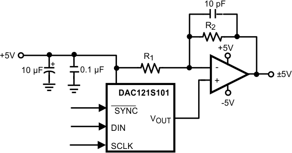
The DAC121S101 is designed for single supply operation and thus has a unipolar output. However, a bipolar output may be obtained with the circuit in Figure 39. This circuit will provide an output voltage range of ±5 V. A rail-to-rail amplifier must be used if the amplifier supplies are limited to ±5 V.
 Figure 39. Bipolar Operation
The output voltage of this circuit for any code is found to be
where
- D is the input code in decimal form.
With VA = 5 V and R1 = R2,
A list of rail-to-rail amplifiers suitable for this application are indicated in Table 2.
Table 2. Some Rail-to-Rail Amplifiers
| AMP | PKGS | Typ VOS | Typ ISUPPLY |
|---|---|---|---|
| LMC7111 | PDIP SOT-23 |
0.9 mV | 25 µA |
| LM7301 | SOIC SOT-23 |
0.03 mV | 620 µA |
| LM8261 | SOT-23 | 0.7 mV | 1 mA |
9.2 Typical Application
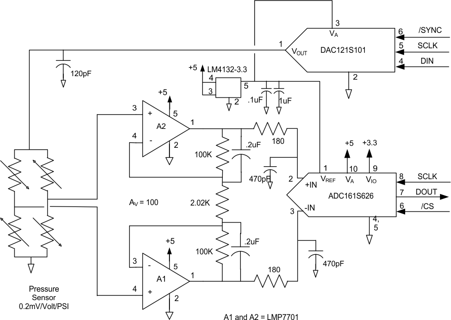
 Figure 40. Pressure Sensor Gain Adjust
9.2.1 Design Requirements
A positive supply only data acquisition system capable of digitizing a pressure sensor output. In addition to digitizing the pressure sensor output, the system designer can use the DAC121S101 to correct for gain errors in the pressure sensor output by adjusting the bias voltage to the bridge pressure sensor.
9.2.2 Detailed Design Procedure
As shown in Equation 4, the output of the pressure sensor is relative to the imbalance of the resistive bridge times the output of the DAC121S101, thus providing the desired gain correction.
Likewise for the ADC161S626, Equation 5 shows that the ADC output is function of the Pressure Sensor Output times relative to the ratio of the ADC input divided by the DAC121S101 output voltage.
9.2.3 Application Curve
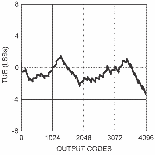
 Figure 41. Total Unadjusted Error vs. Output Code