ZHCS597B December 2011 – May 2015 DAC1282
PRODUCTION DATA.
- 1 特性
- 2 应用
- 3 说明
- 4 修订历史记录
- 5 Device Comparison
- 6 Pin Configuration and Functions
- 7 Specifications
-
8 Detailed Description
- 8.1 Overview
- 8.2
Feature Description
- 8.2.1 Signal Output (VOUTP, VOUTN)
- 8.2.2 DAC Modes
- 8.2.3 Reference Voltage (VREF)
- 8.2.4 Output Filter (CAPP, CAPN)
- 8.2.5 Output Switch (SWINP, SWINN, SWOUTP, SWOUTN)
- 8.2.6 Clock Input (CLK)
- 8.2.7 Switch Control/External Digital Input (SW/TD)
- 8.2.8 SYNC
- 8.2.9 RESET/PWDN
- 8.2.10 AVDD, AVSS, and DVDD Power Supplies
- 8.2.11 Step Response
- 8.2.12 Frequency Response
- 8.3 Device Functional Modes
- 8.4 Programming
- 8.5 Register Map
- 9 Application and Implementation
- 10器件和文档支持
- 11机械、封装和可订购信息
7 Specifications
7.1 Absolute Maximum Ratings(1)
Over operating free-air temperature range, unless otherwise noted.| MIN | MAX | UNIT | |||
|---|---|---|---|---|---|
| AVDD to AVSS | –0.3 | +5.5 | V | ||
| AVSS to DGND | –2.8 | +0.3 | V | ||
| DVDD to DGND | –0.3 | +3.6 | V | ||
| Input current continuous | –10 | +10 | mA | ||
| Analog input/output voltage | AVSS – 0.3 | AVDD + 0.3 | V | ||
| Switch current | –60 | +60 | mA | ||
| Digital input voltage to DGND | –0.3 | DVDD + 0.3 | V | ||
| Operating temperature range | –50 | +125 | °C | ||
| Storage temperature, Tstg | –60 | +150 | °C | ||
(1) Stresses above these ratings may cause permanent damage. Exposure to absolute maximum conditions for extended periods may degrade device reliability. These are stress ratings only, and functional operation of the device at these or any other conditions beyond those specified is not implied.
7.2 ESD Ratings
| VALUE | UNIT | |||
|---|---|---|---|---|
| V(ESD) | Electrostatic discharge | Human-body model (HBM), per ANSI/ESDA/JEDEC JS-001(1) | ±2000 | V |
| Charged-device model (CDM), per JEDEC specification JESD22-C101(2) | ±500 | |||
(1) JEDEC document JEP155 states that 500-V HBM allows safe manufacturing with a standard ESD control process.
(2) JEDEC document JEP157 states that 250-V CDM allows safe manufacturing with a standard ESD control process.
7.3 Thermal Information
| THERMAL METRIC(1) | PW (TSSOP) | UNIT | |
|---|---|---|---|
| 24 PINS | |||
| RθJA | Junction-to-ambient thermal resistance | 78.3 | °C/W |
| RθJC(top) | Junction-to-case (top) thermal resistance | 12.1 | |
| RθJB | Junction-to-board thermal resistance | 33.8 | |
| ψJT | Junction-to-top characterization parameter | 0.3 | |
| ψJB | Junction-to-board characterization parameter | 33.5 | |
| RθJC(bot) | Junction-to-case (bottom) thermal resistance | N/A | |
(1) For more information about traditional and new thermal metrics, see the IC Package Thermal Metrics application report, SPRA953.
7.4 Electrical Characteristics
Minimum and maximum specifications are at TA = –40°C to +85°C. Typical specifications are at TA = +25°C, AVDD = +2.5 V, AVSS = –2.5 V, fCLK = 4.096 MHz, VREF = 5 V, and DVDD = 3.3 V (unless otherwise noted). Refer to Figure 50. DAC1282A supports gains = 1/1, 1/4, and 1/16 only.| PARAMETER | TEST CONDITIONS | MIN | TYP | MAX | UNIT | ||
|---|---|---|---|---|---|---|---|
| ANALOG OUTPUT (VOUTP, VOUTN) | |||||||
| Full-scale output voltage(1) | Gain = 1/1 to 1/64 | ±VREF /2 × gain | V | ||||
| Output common-mode voltage(2) | –0.1 | V | |||||
| Differential output impedance | 1.6 | Ω | |||||
| CLOAD | Capacitive load | 2 | nF | ||||
| RLOAD | Resistive load | 100 | Ω | ||||
| Output current limit(3) | ±60 | mA | |||||
| High-Z output leakage | TA = +25°C | 2 | nA | ||||
| TA = +85°C | 50 | ||||||
| DC PERFORMANCE (Excluding Pulse Mode) | |||||||
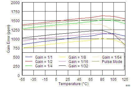
| Gain error | Gain = 1/1 | ±0.1% | ±0.75% | ||||
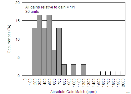
| Gain match | Relative to gain = 1/1 | ±0.05% | ±0.5% | ||||
| Gain drift | 2 | ppm/°C | |||||
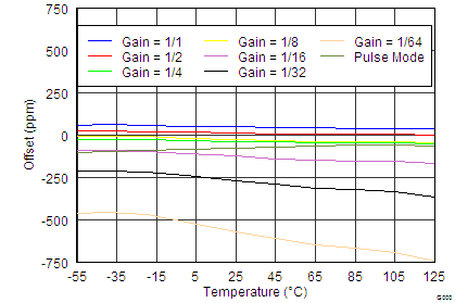
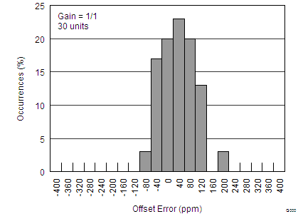
| Offset | Gain = 1/1 to 1/64 | ±(7/gain) + 50 | ±(75/gain) + 300 | ppm FSR(4) | |||
| Offset drift | 1.5 | ppm FSR/°C | |||||
| AC PERFORMANCE | |||||||
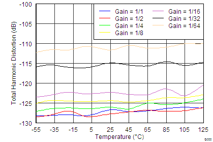
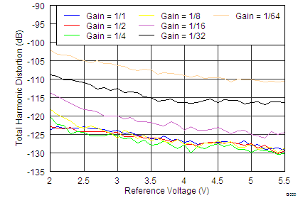
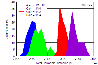
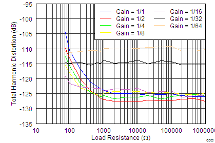
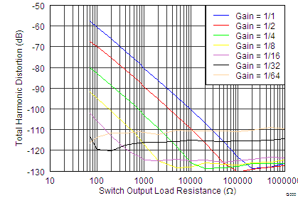
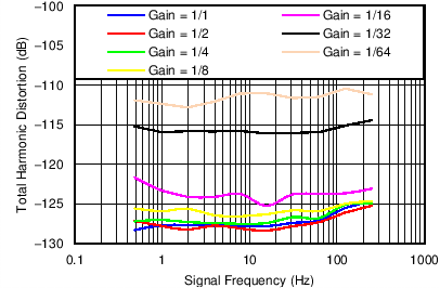
| THD | Total harmonic distortion(8) | DAC1282 | Gain = 1/1 | –125 | –118 | dB | |
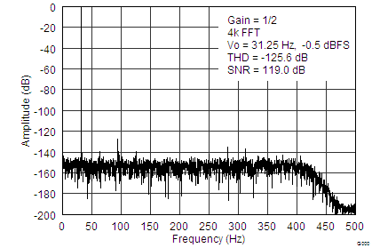
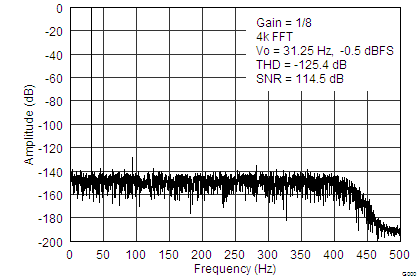
| Gain = 1/2, 1/4, 1/8 | –125 | dB | |||||
| Gain = 1/16 | –123 | dB | |||||
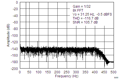
| Gain = 1/32 | –115 | dB | |||||
| Gain = 1/64 | –111 | dB | |||||
| DAC1282A | Gain = 1/1 | –118 | –106 | dB | |||
| Gain = 1/4, 1/16 | –118 | dB | |||||
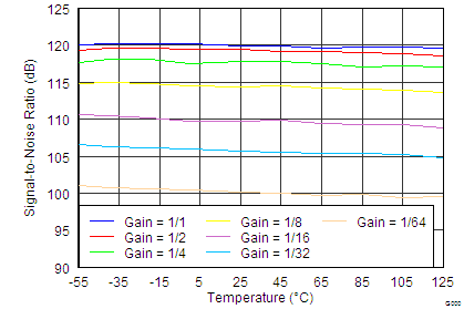
| SNR | Signal-to-noise ratio(7) | Gain = 1/1 | 116 | 120 | dB | ||
| Gain = 1/2 | 119 | dB | |||||
| Gain = 1/4 | 117 | dB | |||||
| Gain = 1/8 | 114 | dB | |||||
| Gain = 1/16 | 110 | dB | |||||
| Gain = 1/32 | 106 | dB | |||||
| Gain = 1/64 | 100 | dB | |||||
| Output frequency | 0.4883 | 250 | Hz | ||||
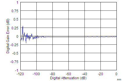
| Digital gain | 0.5-dB steps | Full mute | 0 | dB | |||
| PSR | Power-supply rejection | AVDD, AVSS | 60-Hz ac, gain = 1/8 | 85 | dB | ||
| DVDD | 120 | dB | |||||
| PULSE MODE | |||||||
| Output levels | 31 steps, approximate 3 dB per step | ±0.0195 | ±2.5 | V | |||
| Gain error | ±0.1% | ±0.75% | |||||
| Gain drift | 3 | ppm/°C | |||||
| Offset | ±0.5 | ±3 | mV | ||||
| Offset drift | 3 | µV/°C | |||||
| Output noise(5) | 1.5 | µVRMS | |||||
| Slew rate | 5 | V/µs | |||||
| Settling time | 0.1% final value | 25 | µs | ||||
| DC MODE | |||||||
| Resolution | 24 | Bits | |||||
| Step response | 100 | µs | |||||
| DC noise(6) | Gain = 1/1 | 1.3 | µVRMS | ||||
| Gain = 1/2 | 1.4 | µVRMS | |||||
| Gain = 1/4 | 1.8 | µVRMS | |||||
| Gain = 1/8 | 2.7 | µVRMS | |||||
| Gain = 1/16 | 4.7 | µVRMS | |||||
| Gain = 1/32 | 8.5 | µVRMS | |||||
| Gain = 1/64 | 16 | µVRMS | |||||
| DIGITAL DATA MODE | |||||||
| Data clock rate | fCLK/16 | Hz | |||||
| Ones-density full-scale modulation | +FS and –FS, respectively | 25% | 75% | ||||
| Signal bandwidth | –3 dB | 8.2 | kHz | ||||
| REFERENCE VOLTAGE INPUT (VREF) | |||||||
| Reference voltage, VREF = VREF – AVSS | 2.4 | 5 | AVDD + 0.25 | V | |||
| Reference input impedance | Operating | 220 | kΩ | ||||
| Power-down | 10 | MΩ | |||||
| SIGNAL SWITCH | |||||||
| Signal range | AVSS | AVDD | V | ||||
| Current | Continuous | ±50 | mA | ||||
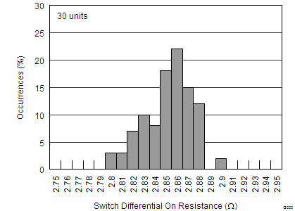
| Differential on-resistance | VSWIN , VSWOUT = 0 V | 2.8 | Ω | ||||
| Differential on-resistance flatness | VSWIN, VSWOUT = AVDD to AVSS | 0.7 | Ω | ||||
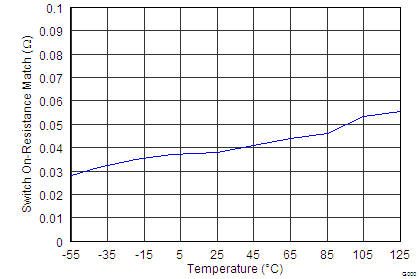
| On-resistance match between outputs | VSWIN , VSWOUT = 0 V | 0.04 | Ω | ||||
| Off-leakage current(10) | TA = +25°C | ±0.1 | nA | ||||
| TA = +85°C | ±5 | ||||||
| Off-isolation(11) | 120 | dB | |||||
| DIGITAL INPUT/OUTPUT (DVDD = 1.65 V to 3.6 V) | |||||||
| VOH | IOH = 1 mA | 0.8 × DVDD | V | ||||
| VOL | IOL = 1 mA | 0.2 × DVDD | V | ||||
| VIH | 0.8 × DVDD | DVDD | V | ||||
| VIL | DGND | 0.2 × DVDD | V | ||||
| Input hysteresis | 0.5 | V | |||||
| Input leakage | ±10 | µA | |||||
| fCLK | CLK Input | 1 | 4.096 | 4.225 | MHz | ||
| POWER SUPPLY | |||||||
| AVSS | –2.6 | 0 | V | ||||
| AVDD | AVSS + 4.75 | AVSS + 5.25 | V | ||||
| DVDD | 1.65 | 3.6 | V | ||||
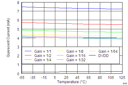
| AVDD, AVSS current | Gain = 1/1, VOUT = 0 V | 7.4 | 8.5 | mA(12) | |||
| Pulse mode, VOUT = 0 V | 7 | mA | |||||
| Shutdown | 1 | 10 | µA | ||||
| DVDD current | Operating | 180 | 300 | µA | |||
| Shutdown(9) | 1 | 10 | µA | ||||
| Power | Operating | 38 | 44 | mW | |||
| Shutdown(9) | 10 | 85 | µW | ||||
| TEMPERATURE RANGE | |||||||
| Specified temperature range | –40 | +85 | °C | ||||
| Operating temperature range | –50 | +125 | °C | ||||
| Storage temperature range | –65 | +150 | °C | ||||
(1) Full-scale differential output voltage: VOUT = (VOUTP – VOUTN) = ±VREF/2 × Gain. Gain is the DAC analog gain.
(2) Output common-mode voltage scales with analog supply voltage: VCOM = 0.48 × (AVDD – AVSS) + AVSS.
(3) Sink or source current limit of VOUTP and VOUTN.
(4) FSR – full-scale range = VREF × gain.
(5) VOUT = 0 V. Pulse mode output noise is measured by the ADS1282, over a 413-Hz bandwidth using ADC gain = 1.
(6) VOUT = 0 V. DC noise is measured by the ADS1282, over a 413-Hz bandwidth using complementing gain. DC noise is referred to a 1.77-V full-scale ADC output. Divide output-referred noise by the ADC gain to yield input-referred noise.
(7) SNR = signal-to-noise ratio. SNR is measured by the ADS1282 over a 413-Hz bandwidth using complementing gain. fOUT = 31.25 Hz and VOUT – 0.5 dBFS.
(8) THD = total harmonic distortion. THD is measured by the ADS1282, and is the sum of first nine harmonics using complementing gain. fOUT = 31.25 Hz, VOUT – 0.5 dBFS, no load.
(9) Digital inputs stopped and maintained at VIH or VIL level.
(10) Switch input or output voltage = AVDD – 0.5 V to AVSS + 0.5 V.
(11) f = 31.25 Hz, 1.77 VRMS. Switch output loaded 2 x 10 kΩ to mid-supply range.
(12) Analog supply current scales with gain as follows:
IAVDD and IAVSS = 0.016 × VREF × (44 × Gain + 1) + 3.8 (mA).
IAVDD and IAVSS = 0.016 × VREF × (44 × Gain + 1) + 3.8 (mA).
7.5 Timing Requirements: Serial Peripheral Interface (SPI) Timing
At TA = –40°C to +85°C and DVDD = 1.65 V to 3.6 V, unless otherwise noted.| MIN | MAX | UNIT | |||
|---|---|---|---|---|---|
| tCSSC | CS low to first SCLK: setup time(1) | 30 | ns | ||
| tSCLK | SCLK period | 120 | ns | ||
| tSPWH | SCLK pulse width: high | 50 | ns | ||
| tSPWL | SCLK pulse width: low(3) | 50 | ns | ||
| 218 | tCLK | ||||
| tDIST | Valid DIN to SCLK high: setup time | 40 | ns | ||
| tDIHD | Valid DIN to SCLK high: hold time | 20 | ns | ||
| tDOPD | SCLK low to valid new DOUT: propagation delay(2) | 40 | ns | ||
| tDOHD | SCLK low to DOUT invalid: hold time | 0 | ns | ||
| tCSDOD | CS low to DOUT driven: propagation delay(2) | 40 | ns | ||
| tCSDOZ | CS high to DOUT Hi-Z: propagation delay | 20 | ns | ||
| tCSH | CS high pulse | 50 | ns | ||
| tSCCS | Last SCLK falling edge to CS high | 0 | ns | ||
(1) CS can be tied low.
(2) DOUT load = 20 pF || 100 kΩ to DGND.
(3) Holding SCLK low longer than 218 fCLK cycles resets the SPI interface.
 Figure 1. Serial Interface Timing
7.6 Typical Characteristics
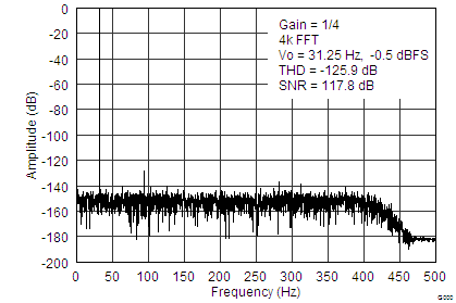
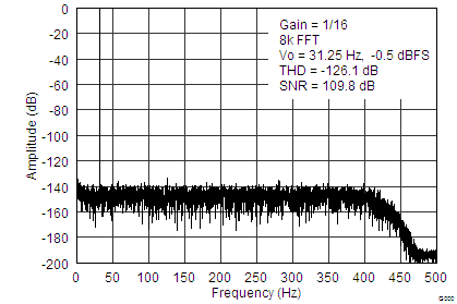
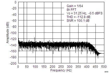
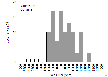
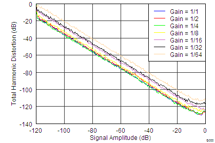
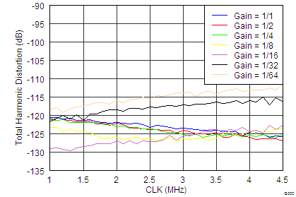
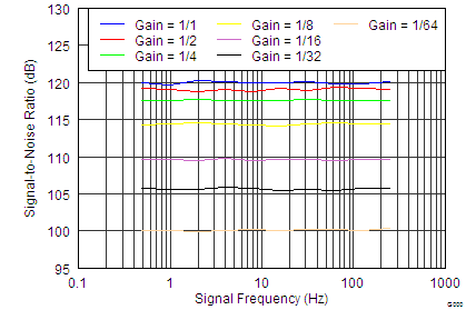
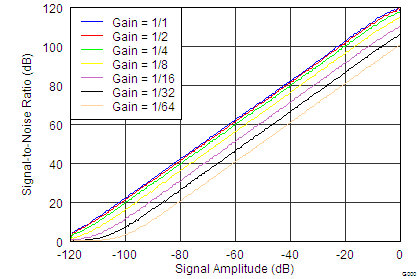
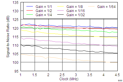
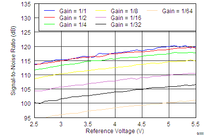
At TA = +25°C, AVDD = +2.5 V, AVSS = –2.5 V, DVDD = 3.3 V, fCLK = 4.096 MHz, and VREF = 5 V, unless otherwise noted. DAC1282A supports gains = 1/1, 1/4, and 1/16 only.
