SNAS515G July   2011  – December 2014 DAC161P997

PRODUCTION DATA.  

  1. Features
  2. Application
  3. Description
  4. Revision History
  5. Pin Configuration and Functions
  6. Specifications
    1. 6.1 Absolute Maximum Ratings
    2. 6.2 ESD Ratings
    3. 6.3 Recommended Operating Conditions
    4. 6.4 Thermal Information
    5. 6.5 Electrical Characteristics
    6. 6.6 Timing Requirements
    7. 6.7 Typical Characteristics
  7. Detailed Description
    1. 7.1 Overview
    2. 7.2 Functional Block Diagram
    3. 7.3 Feature Description
      1. 7.3.1 Error Detection and Reporting
      2. 7.3.2 Alarm Current
    4. 7.4 Device Functional Modes
    5. 7.5 Programming
      1. 7.5.1 Single-Wire Interface (SWIF)
        1. 7.5.1.1 Frame Format
        2. 7.5.1.2 Inter-Frame Period
        3. 7.5.1.3 Symbol Set
        4. 7.5.1.4 Interface Circuit
          1. 7.5.1.4.1 Transformer Coupled Interface - Data Flow to the DAC
          2. 7.5.1.4.2 Transformer Coupled Interface - Acknowledge Pulse
          3. 7.5.1.4.3 DC-Coupled Interface
          4. 7.5.1.4.4 Transformer Selection and SWIF Data Link Circuit Design
    6. 7.6 Register Maps
      1. 7.6.1 LCK
      2. 7.6.2 CONFIG1
      3. 7.6.3 CONFIG2
      4. 7.6.4 CONFIG3
      5. 7.6.5 ERR_LOW
      6. 7.6.6 ERR_HIGH
  8. Application and Implementation
    1. 8.1 Application Information
      1. 8.1.1 16-BIT DAC and Loop Drive
        1. 8.1.1.1 DC Characteristics
          1. 8.1.1.1.1 DC Input-Output Transfer Function
          2. 8.1.1.1.2 Loop Interface
          3. 8.1.1.1.3 Loop Compliance
        2. 8.1.1.2 AC Characteristics
          1. 8.1.1.2.1 Step Response
          2. 8.1.1.2.2 Output Impedance
          3. 8.1.1.2.3 PSRR
          4. 8.1.1.2.4 Stability
          5. 8.1.1.2.5 Noise and Ripple
          6. 8.1.1.2.6 Digital Feedthrough
          7. 8.1.1.2.7 HART Signal Injection
          8. 8.1.1.2.8 RC Filter Limitation
    2. 8.2 Typical Application
      1. 8.2.1 Design Requirements
      2. 8.2.2 Detailed Design Procedure
      3. 8.2.3 Application Curve
  9. Power Supply Recommendations
  10. 10Layout
    1. 10.1 Layout Guidelines
    2. 10.2 Layout Example
  11. 11Device and Documentation Support
    1. 11.1 Third-Party Products Disclaimer
    2. 11.2 Trademarks
    3. 11.3 Electrostatic Discharge Caution
    4. 11.4 Glossary
  12. 12Mechanical, Packaging, and Orderable Information

封装选项

机械数据 (封装 | 引脚)
散热焊盘机械数据 (封装 | 引脚)
订购信息

10 Layout

10.1 Layout Guidelines

To maximize the performance of the DAC161S997 in any application, good layout practices and proper circuit design must be followed. A few recommendations specific to the DAC161S997 are:

  • Make sure that VD and VA have decoupling capacitors local to the respective terminals.
  • Minimize trace length between the C1, C2, and C3 capacitors and the DAC161S997 pins.
10.2 Layout Example

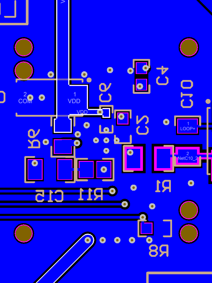
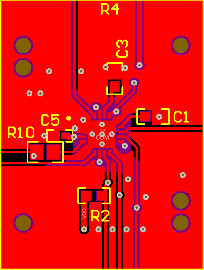
Figure 34 and Figure 35 show the DAC161S997 evaluation module (EVM) layout

lay01_top_snas515.pngFigure 34. Example PCB layout: Top Layer
lay02_bot_snas515.pngFigure 35. Example PCB layout: Bottom Layer