SNAS515G July   2011  – December 2014 DAC161P997

PRODUCTION DATA.  

  1. Features
  2. Application
  3. Description
  4. Revision History
  5. Pin Configuration and Functions
  6. Specifications
    1. 6.1 Absolute Maximum Ratings
    2. 6.2 ESD Ratings
    3. 6.3 Recommended Operating Conditions
    4. 6.4 Thermal Information
    5. 6.5 Electrical Characteristics
    6. 6.6 Timing Requirements
    7. 6.7 Typical Characteristics
  7. Detailed Description
    1. 7.1 Overview
    2. 7.2 Functional Block Diagram
    3. 7.3 Feature Description
      1. 7.3.1 Error Detection and Reporting
      2. 7.3.2 Alarm Current
    4. 7.4 Device Functional Modes
    5. 7.5 Programming
      1. 7.5.1 Single-Wire Interface (SWIF)
        1. 7.5.1.1 Frame Format
        2. 7.5.1.2 Inter-Frame Period
        3. 7.5.1.3 Symbol Set
        4. 7.5.1.4 Interface Circuit
          1. 7.5.1.4.1 Transformer Coupled Interface - Data Flow to the DAC
          2. 7.5.1.4.2 Transformer Coupled Interface - Acknowledge Pulse
          3. 7.5.1.4.3 DC-Coupled Interface
          4. 7.5.1.4.4 Transformer Selection and SWIF Data Link Circuit Design
    6. 7.6 Register Maps
      1. 7.6.1 LCK
      2. 7.6.2 CONFIG1
      3. 7.6.3 CONFIG2
      4. 7.6.4 CONFIG3
      5. 7.6.5 ERR_LOW
      6. 7.6.6 ERR_HIGH
  8. Application and Implementation
    1. 8.1 Application Information
      1. 8.1.1 16-BIT DAC and Loop Drive
        1. 8.1.1.1 DC Characteristics
          1. 8.1.1.1.1 DC Input-Output Transfer Function
          2. 8.1.1.1.2 Loop Interface
          3. 8.1.1.1.3 Loop Compliance
        2. 8.1.1.2 AC Characteristics
          1. 8.1.1.2.1 Step Response
          2. 8.1.1.2.2 Output Impedance
          3. 8.1.1.2.3 PSRR
          4. 8.1.1.2.4 Stability
          5. 8.1.1.2.5 Noise and Ripple
          6. 8.1.1.2.6 Digital Feedthrough
          7. 8.1.1.2.7 HART Signal Injection
          8. 8.1.1.2.8 RC Filter Limitation
    2. 8.2 Typical Application
      1. 8.2.1 Design Requirements
      2. 8.2.2 Detailed Design Procedure
      3. 8.2.3 Application Curve
  9. Power Supply Recommendations
  10. 10Layout
    1. 10.1 Layout Guidelines
    2. 10.2 Layout Example
  11. 11Device and Documentation Support
    1. 11.1 Third-Party Products Disclaimer
    2. 11.2 Trademarks
    3. 11.3 Electrostatic Discharge Caution
    4. 11.4 Glossary
  12. 12Mechanical, Packaging, and Orderable Information

封装选项

机械数据 (封装 | 引脚)
散热焊盘机械数据 (封装 | 引脚)
订购信息

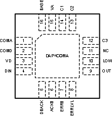
5 Pin Configuration and Functions

WQFN (RGH0016A)
16 pins
Top View
30154403.gif

Pin Functions

PIN DESCRIPTION ESD PROTECTION
NAME NO.
VA 15 Analog block positive supply rail
30154404.gif
COMA 1 Analog block negative supply rail (local COMMMON)
30154405.gif
COMD 2 Digital block negative supply rail (local COMMON)
30154406.gif
VD 3 Digital block positive supply rail
30154407.gif
DIN 4 SWIF input
DBACK 5 SWIF input loop back
ACKB 6 SWIF acknowledge output - open drain, active LOW
ERRLVL 8 Sets the output current level at power-up
LOW 10 Must be tied to COMA, COMD potential
C1 14 External capacitor
C2 13 External capacitor, HART Input
C3 12 External capacitor
BASE 16 External NPN base drive
N.C. 11 User must not connect to this pin
ERRB 7 Error flag output open drain, active LOW
30154408.gif
OUT 9 Loop output current source
30154409.gif
DAP - Die Attach Pad. For best thermal conductivity and best noise immunity DAP should be soldered to the PCB pad which is connected directly to circuit common node (COMA, COMD) -