SLAS646C December 2009 – May 2015 DAC3282
PRODUCTION DATA.
- 1 Features
- 2 Applications
- 3 Description
- 4 Revision History
- 5 Pin Configuration and Functions
-
6 Specifications
- 6.1 Absolute Maximum Ratings
- 6.2 ESD Ratings
- 6.3 Recommended Operating Conditions
- 6.4 Thermal Information
- 6.5 Electrical Characteristics - DC Specifications
- 6.6 Electrical Characteristics - AC Specifications
- 6.7 Electrical Characteristics - Digital Specifications
- 6.8 Timing Characteristics
- 6.9 Typical Characteristics
-
7 Detailed Description
- 7.1 Overview
- 7.2 Functional Block Diagram
- 7.3
Feature Description
- 7.3.1 Input FIFO
- 7.3.2 FIFO Alarms
- 7.3.3 FIFO Modes of Operation
- 7.3.4 Dual Sync Sources Mode
- 7.3.5 Single Sync Source Mode
- 7.3.6 Bypass Mode
- 7.3.7 Data Pattern Checker
- 7.3.8 FIR Filters
- 7.3.9 Coarse Mixer
- 7.3.10 Digital Offset Control
- 7.3.11 Temperature Sensor
- 7.3.12 Sleep Modes
- 7.3.13 Reference Operation
- 7.4 Device Functional Modes
- 7.5 Programming
- 7.6
Register Maps
- 7.6.1 CONFIG0 (address = 0x00) [reset = 0x70]
- 7.6.2 CONFIG1 (address = 0x01) [reset = 0x11]
- 7.6.3 CONFIG2 (address = 0x02) [reset = 0x00]
- 7.6.4 CONFIG3 (address = 0x03) [reset = 0x10]
- 7.6.5 CONFIG4 (address = 0x04) [reset = 0xFF]
- 7.6.6 CONFIG5 (address = 0x05) READ ONLY
- 7.6.7 CONFIG6 (address =0x06) [reset = 0x00]
- 7.6.8 CONFIG7 (address = 0x07) [reset = 0x00] (WRITE TO CLEAR)
- 7.6.9 CONFIG8 (address = 0x08) [reset = 0x00] (WRITE TO CLEAR)
- 7.6.10 CONFIG9 (address = 0x09) [reset = 0x7A]
- 7.6.11 CONFIG10 (address = 0x0A) [reset = 0xB6]
- 7.6.12 CONFIG11 (address = 0x0B) [reset = 0xEA]
- 7.6.13 CONFIG12 (address =0x0C) [reset = 0x45]
- 7.6.14 CONFIG13 (address =0x0D) [reset = 0x1A]
- 7.6.15 CONFIG14 Register Name (address = 0x0E) [reset = 0x16]
- 7.6.16 CONFIG15 Register Name (address = 0x0F) [reset = 0xAA]
- 7.6.17 CONFIG16 (address = 0x10) [reset = 0xC6]
- 7.6.18 CONFIG17 (address = 0x11) [reset = 0x00]
- 7.6.19 CONFIG18 (address = 0x12) [reset = 0x02]
- 7.6.20 CONFIG19 (address = 0x13) [reset = 0x00]
- 7.6.21 CONFIG20 (address = 0x14) [reset = 0x00] (CAUSES AUTOSYNC)
- 7.6.22 CONFIG21 (address = 0x15) [reset = 0x00]
- 7.6.23 CONFIG22 (address = 0x16) [reset = 0x00]
- 7.6.24 CONFIG23 (address = 0x17) [reset = 0x00]
- 7.6.25 CONFIG24 (address = 0x18) [reset = 0x83]
- 7.6.26 CONFIG25 (address = 0x19) [reset = 0x00]
- 7.6.27 CONFIG26 (address = 0x1A) [reset = 0x00]
- 7.6.28 CONFIG27 (address =0x1B) [reset = 0x00]
- 7.6.29 CONFIG28 (address = 0x1C) [reset = 0x00]
- 7.6.30 CONFIG29 (address = 0x1D) [reset = 0x00]
- 7.6.31 CONFIG30 (address = 0x1E) [reset = 0x00]
- 7.6.32 VERSION31 (address = 0x1F) [reset = 0x43] (READ ONLY)
- 8 Application and Implementation
- 9 Power Supply Recommendations
- 10Layout
- 11Device and Documentation Support
- 12Mechanical, Packaging, and Orderable Information
8 Application and Implementation
NOTE
Information in the following applications sections is not part of the TI component specification, and TI does not warrant its accuracy or completeness. TI’s customers are responsible for determining suitability of components for their purposes. Customers should validate and test their design implementation to confirm system functionality.
8.1 Application Information
The DAC3282 is appropriate for a variety of transmitter applications including complex I/Q direct conversion, up-conversion using an intermediate frequency (IF) and diversity applications.
8.1.1 Multi-device Synchronization
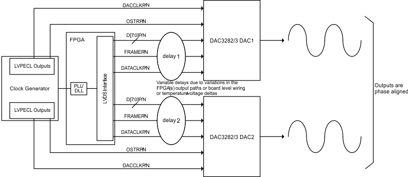
In various applications, such as multi antenna systems where the various transmit channels information is correlated, it is required that multiple DAC devices are completely synchronized such that their outputs are phase aligned. The DAC3282 architecture supports this mode of operation.
8.1.1.1 Multi-device Synchronization: Dual Sync Sources Mode
For single or multi-device synchronization it is important that delay differences in the data are absorbed by the device so that latency through the device remains the same. Furthermore, to guarantee that the outputs from each DAC are phase aligned it is necessary that data is read from the FIFO of each device simultaneously. In the DAC3282 this is accomplished by operating the multiple devices in Dual Sync Sources mode. In this mode the additional OSTR signal is required by each DAC3282 to be synchronized.
Data into the device is input as LVDS signals from one or multiple baseband ASICs or FPGAs. Data into the multiple DAC devices can experience different delays due to variations in the digital source output paths or board level wiring. These different delays can be effectively absorbed by the DAC3282 FIFO so that all outputs are phase aligned correctly.
For correct operation both OSTR and DACCLK must be generated from the same clock domain. The OSTR signal is sampled by DACCLK and must satisfy the timing requirements in the specifications table. If the clock generator does not have the ability to delay the DACCLK to meet the OSTR timing requirement, the polarity of the DACCLK outputs can be swapped with respect to the OSTR ones to create 180 degree phase delay of the DACCLK. This may help establish proper setup and hold time requirement of the OSTR signal.
Careful board layout planning must be done to ensure that the DACCLK and OSTR signals are distributed from device to device with the lowest skew possible as this will affect the synchronization process. In order to minimize the skew across devices it is recommended to use the same clock distribution device to provide the DACCLK and OSTR signals to all the DAC devices in the system.
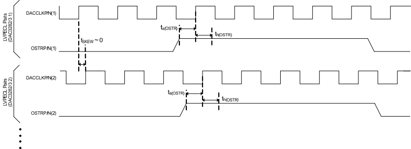 Figure 75. Timing Diagram for LVPECL Synchronization Signals
The following steps are required to ensure the devices are fully synchronized. The procedure assumes all the DAC3282 devices have a DACCLK and OSTR signal and must be carried out on each device.
- Start-up the device as described in the power-up sequence. Set the DAC3282 in Dual Sync Sources mode and select OSTR as the FIFO output pointer sync source and clock divider sync source (multi_sync_sel in register config19).
- Sync the clock divider and FIFO pointers.
- Verify there are no FIFO alarms either through register config7 or through the ALARM_SDO pin.
After these steps all the DAC3282 outputs will be synchronized.
8.1.1.2 Multi-device Operation: Single Sync Source Mode
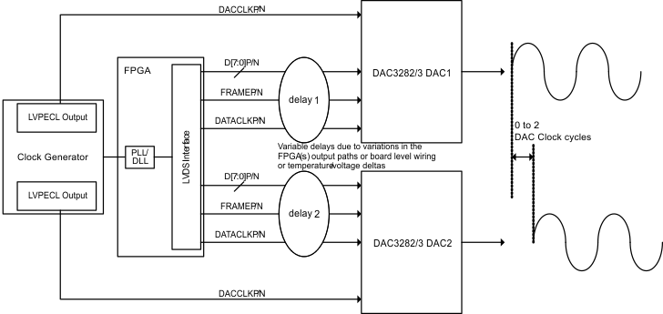
In Single Sync Source mode, the FIFO write and read pointers are reset from the same FRAME source. Although the FIFO in this mode can still absorb the data delay differences due to variations in the digital source output paths or board level wiring, it is impossible to guarantee data will be read from the FIFO of different devices simultaneously thus preventing exact phase alignment.
The FIFO read pointer reset is handoff between the two clock domains (DATACLK and FIFO OUT CLOCK) by simply re-sampling the write pointer reset. Since the two clocks are asynchronous there is a small but distinct possibility of a meta-stablility during the pointer handoff. This meta-stability can cause the outputs of the multiple devices to slip by up to 2 DAC clock cycles.
8.1.2 Analog Current Outputs
Figure 77 shows a simplified schematic of the current source array output with corresponding switches. Differential switches direct the current of each individual NMOS current source to either the positive output node IOUT1 or its complementary negative output node IOUT2. The output impedance is determined by the stack of the current sources and differential switches, and is typically >300 kΩ in parallel with an output capacitance of 5 pF.
The external output resistors are referred to an external ground. The minimum output compliance at nodes IOUT1 and IOUT2 is limited to AVDD – 0.5 V, determined by the CMOS process. Beyond this value, transistor breakdown may occur resulting in reduced reliability of the DAC3282 device. The maximum output compliance voltage at nodes IOUT1 and IOUT2 equals AVDD + 0.5 V. Exceeding the minimum output compliance voltage adversely affects distortion performance and integral non-linearity. The optimum distortion performance for a single-ended or differential output is achieved when the maximum full-scale signal at IOUT1 and IOUT2 does not exceed 0.5 V.
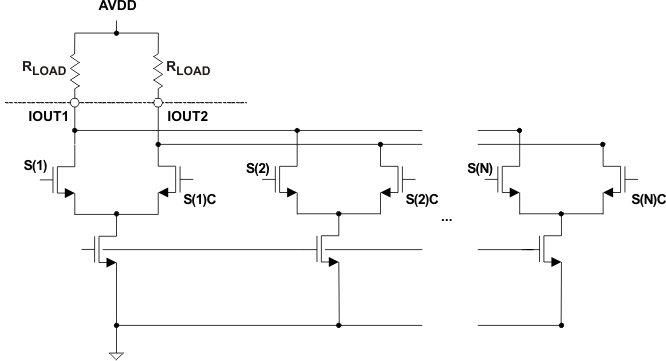 Figure 77. Equivalent Analog Current Output
The DAC3282 can be easily configured to drive a doubly terminated 50 Ω cable using a properly selected RF transformer. Figure 78 and Figure 79 show the 50 Ω doubly terminated transformer configuration with 1:1 and 4:1 impedance ratio, respectively. Note that the center tap of the primary input of the transformer has to be connected to AVDD to enable a DC current flow. Applying a 20 mA full-scale output current would lead to a 0.5 Vpp for a 1:1 transformer and a 1 Vpp output for a 4:1 transformer. The low dc-impedance between IOUT1 or IOUT2 and the transformer center tap sets the center of the ac-signal at AVDD, so the 1 Vpp output for the 4:1 transformer results in an output between AVDD + 0.5 V and AVDD – 0.5 V.
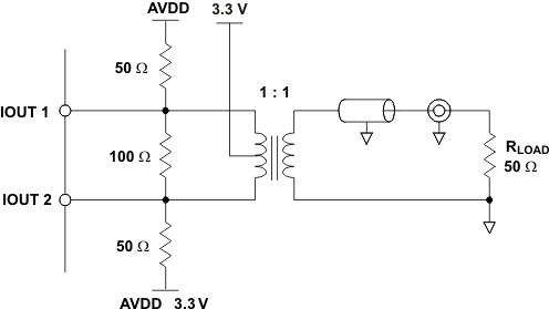 Figure 78. Driving a Doubly Terminated 50 Ω Cable Using a 1:1 Impedance Ratio Transformer
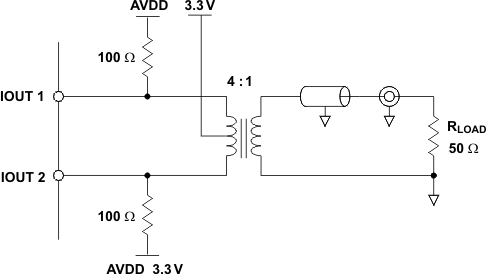 Figure 79. Driving a Doubly Terminated 50 Ω Cable Using a 4:1 Impedance Ratio Transformer
8.1.3 Passive Interface to Analog Quadrature Modulators
A common application in communication systems is to interface the DAC to an IQ modulator like the TRF3703 family of modulators from Texas Instruments. The input of the modulator is generally of high impedance and requires a specific common-mode voltage. A simple resistive network can be used to maintain 50Ω load impedance for the DAC3282 and also provide the necessary common-mode voltages for both the DAC and the modulator.
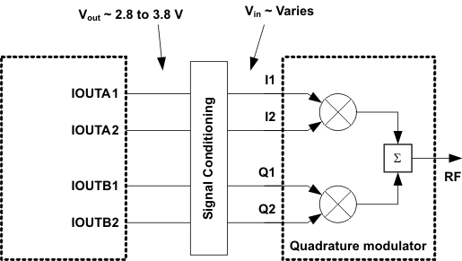 Figure 80. DAC to Analog Quadrature Modulator Interface
The DAC3282 has a maximum 20mA full-scale output and a voltage compliance range of AVDD ± 0.5 V. The TRF3703 IQ modulator family can be operated at three common-mode voltages: 1.5V, 1.7V, and 3.3V.
Figure 81 shows the recommended passive network to interface the DAC3282 to the TRF3703-17 which has a common mode voltage of 1.7V. The network generates the 3.3V common mode required by the DAC output and 1.7V at the modulator input, while still maintaining 50Ω load for the DAC.
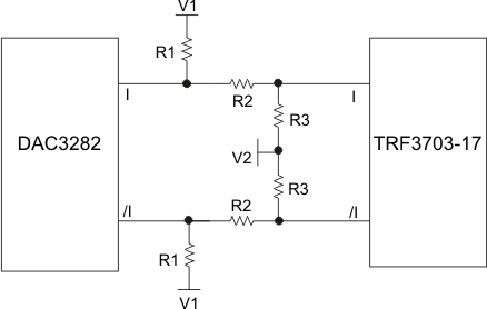 Figure 81. DAC3282 to TRF3703-17 Interface
If V1 is set to 5V and V2 is set to -5V, the corresponding resistor values are R1 = 57Ω, R2 = 80Ω, and R3 = 336Ω. The loss developed through R2 is about -1.86 dB. In the case where there is no –5V supply available and V2 is set to 0V, the resistor values are R1 = 66Ω, R2 = 101Ω, and R3 = 107Ω. The loss with these values is –5.76dB.
Figure 82 shows the recommended network for interfacing with the TRF3703-33 which requires a common mode of 3.3V. This is the simplest interface as there is no voltage shift. Because there is no voltage shift there isn't any loss in the network. With V1 = 5V and V2 = 0V, the resistor values are R1 = 66Ω and R3 = 208Ω.
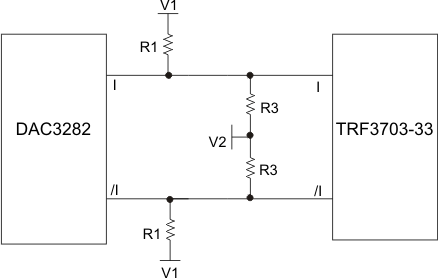 Figure 82. DAC3282 to TRF3703-33 Interface
In most applications a baseband filter is required between the DAC and the modulator to eliminate the DAC images. This filter can be placed after the common-mode biasing network. For the DAC to modulator network shown in Figure 83, R2 and the filter load R4 need to be considered into the DAC impedance. The filter has to be designed for the source impedance created by the resistor combination of R3 // (R2+R1). The effective impedance seen by the DAC is affected by the filter termination resistor resulting in R1 // (R2+R3 // (R4/2)).
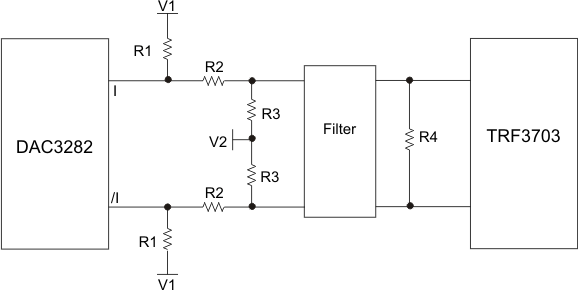 Figure 83. DAC3282 to Modulator Interface with Filter
Factoring in R4 into the DAC load, a typical interface to the TRF3703-17 with V1 = 5V and V2 = 0V results in the following values: R1 = 72Ω, R2 = 116Ω, R3 = 124Ω and R4 = 150Ω. This implies that the filter needs to be designed for 75Ω input and output impedance (single-ended impedance). The common mode levels for the DAC and modulator are maintained at 3.3V and 1.7V and the DAC load is 50Ω. The added load of the filter termination causes the signal to be attenuated by –10.8 dB.
A filter can be implemented in a similar manner to interface with the TRF3703-33. In this case it is much simpler to balance the loads and common mode voltages due to the absence of R2. An added benefit is that there is no loss in this network. With V1 = 5V and V2 = 0V the network can be designed such that R1 = 115Ω, R3 = 681Ω, and R4 = 200Ω. This results in a filter impedance of R1 // R2=100Ω, and a DAC load of R1 // R3 // (R4/2) which is equal to 50Ω. R4 is a differential resistor and does not affect the common mode level created by R1 and R3. The common-mode voltage is set at 3.3 V for a full-scale current of 20mA.
For more information on how to interface the DAC3282 to an analog quadrature modulator please refer to the application reports Passive Terminations for Current Output DACs (SLAA399) and Design of Differential Filters for High-Speed Signal Chains (SLWA053).
8.2 Typical Application
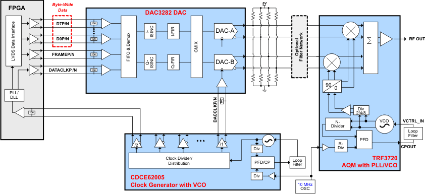 Figure 84. System Diagram of Direct Conversion Radio
8.2.1 Design Requirements
For this design example of a direct conversion transmitter, use the parameters in Table 41.
Table 41. Design Parameters
| PARAMETER | VALUE |
|---|---|
| Channel Type | 4x W-CDMA Carriers, each with 3.84 MHz bandwidth (20 MHz total bandwidth) |
| Input Data Rate | 307.2 MSPS |
| Interpolation | 2 |
| NCO Frequency | Bypassed |
| Output IF | None (Complex baseband) |
| DAC Conversion Rate (DACCLK frequency) | 614.4 MSPS |
8.2.2 Detailed Design Procedure
Refer to Figure 84 for an example Direct Conversion Radio. The DAC3282 receives an interleaved complex I/Q baseband input data stream and increases the sample rate through interpolation by a factor of 2 or 4. By performing digital interpolation on the input data, undesired images of the original signal can be push out of the band of interest and more easily suppressed with analog filters.
For a Zero IF (ZIF) frequency plan, complex mixing of the baseband signal is not required. Alternatively, for a Complex IF frequency plan the input data can be pre-placed at an IF within the bandwidth limitations of the interpolation filters. In addition, complex mixing is available using the coarse mixer block to up-convert the signal. The output of both DAC channels is used to produce a Hilbert transform pair and can be expressed as:
where m(t) and mh(t) connote a Hilbert transform pair and ωc is the mixer frequency. The complex output is input to an analog quadrature modulator (AQM) such as the Texas Instruments TRF3720 for a single side-band (SSB) up conversion to RF. A passive (resistor only) interface to the AQM with an optional LC filter network is recommended. The TRF3720 includes a VCO/PLL to generate the LO frequency. Upper single-sideband upconversion is achieved at the output of the analog quadrature modulator, whose output is expressed as:
Flexibility is provided to the user by allowing for the selection of negative mixing frequency to produce a lower-sideband upconversion. Note that the process of complex mixing translates the signal frequency from 0Hz means that the analog quadrature modulator IQ imbalance produces a sideband that falls outside the signal of interest. DC offset error in DAC and AQM signal path may produce LO feed-through at the RF output which may fall in the band of interest. To suppress the LO feed-through, the DAC3282 provides a digital offset correction capability for both DAC-A and DAC-B paths. In addition phase and gain imbalances in the DAC and AQM result in a lower-sideband product. The DAC3282 offers gain and phase correction capabilities to minimize the sideband product.
The complex IF architecture has several advantages over the real IF architecture:
- Uncalibrated side-band suppression ~ 35dBc compared to 0dBc for real IF architecture.
- Direct DAC to AQM interface – no amplifiers required
- DAC 2nd Nyquist zone image is offset fDAC compared with fDAC– 2 x IF for a real IF architecture, reducing the need for filtering at the DAC output.
- Uncalibrated LO feed through for AQM is ~ 35 dBc and calibration can reduce or completely remove the LO feed through.
8.2.3 Application Performance Curves
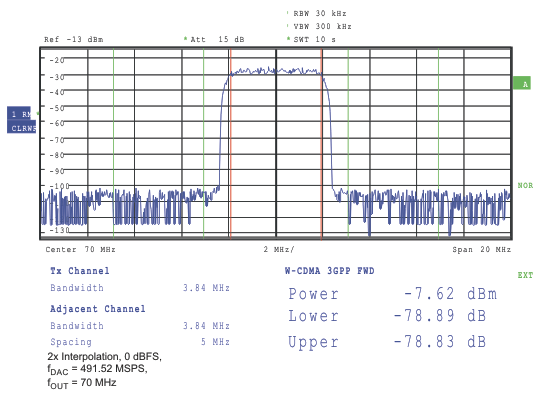 Figure 85. Single Carrier W-CDMA Test Model 1, fOUT = 70 MHz
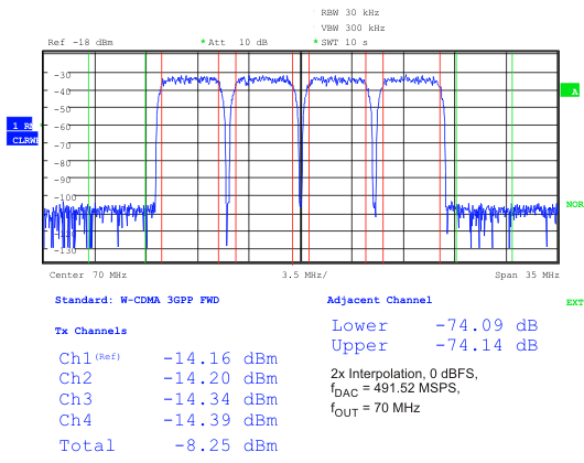 Figure 87. Four Carrier W-CDMA Test Model 1, fOUT = 70 MHz
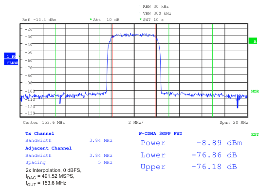 Figure 86. Single Carrier W-CDMA Test Model 1,
 fOUT = 153.6 MHz
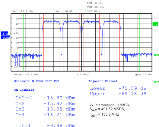 Figure 88. Four Carrier W-CDMA Test Model 1, fOUT = 153.6 MHz
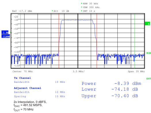 Figure 89. 10MHz Single Carrier LTE, fOUT = 70 MHz
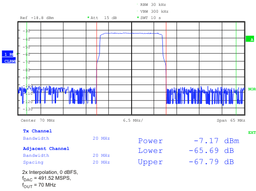 Figure 91. 20MHz Single Carrier LTE, fOUT = 70 MHz
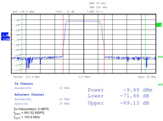 Figure 90. 10MHz Single Carrier LTE, fOUT = 153.6 MHz
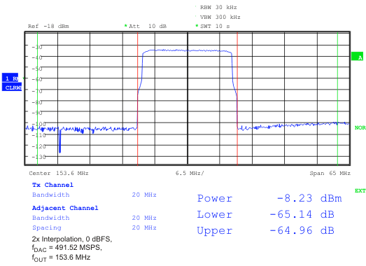 Figure 92. 20MHz Single Carrier LTE, fOUT = 153.6 MHz
