SLAS693C March 2010 – March 2015 DAC3283
PRODUCTION DATA.
- 1 Features
- 2 Applications
- 3 Description
- 4 Simplified Schematic
- 5 Revision History
- 6 Pin Configuration and Functions
-
7 Specifications
- 7.1 Absolute Maximum Ratings
- 7.2 ESD Ratings
- 7.3 Recommended Operating Conditions
- 7.4 Thermal Information
- 7.5 Electrical Characteristics - DC Specifications
- 7.6 Electrical Characteristics - AC Specifications
- 7.7 Electrical Characteristics - Digital Specifications
- 7.8 Timing Requirements
- 7.9 Typical Characteristics
-
8 Detailed Description
- 8.1 Overview
- 8.2 Functional Block Diagram
- 8.3
Feature Description
- 8.3.1
Definition Of Specifications
- 8.3.1.1 Adjacent Carrier Leakage Ratio (ACLR)
- 8.3.1.2 Analog and Digital Power Supply Rejection Ratio (APSSR, DPSSR)
- 8.3.1.3 Differential Nonlinearity (DNL)
- 8.3.1.4 Gain Drift
- 8.3.1.5 Gain Error
- 8.3.1.6 Integral Nonlinearity (INL)
- 8.3.1.7 Intermodulation Distortion (IMD3, IMD)
- 8.3.1.8 Offset Drift
- 8.3.1.9 Offset Error
- 8.3.1.10 Output Compliance Range
- 8.3.1.11 Reference Voltage Drift
- 8.3.1.12 Spurious Free Dynamic Range (SFDR)
- 8.3.1.13 Noise Spectral Density (NSD)
- 8.3.1
Definition Of Specifications
- 8.4
Device Functional Modes
- 8.4.1 Serial Interface
- 8.4.2 Data Interface
- 8.4.3 Input FIFO
- 8.4.4 FIFO Alarms
- 8.4.5 FIFO Modes of Operation
- 8.4.6 Multi-Device Operation
- 8.4.7 Data Pattern Checker
- 8.4.8 DATACLK Monitor
- 8.4.9 FIR Filters
- 8.4.10 Coarse Mixer
- 8.4.11 Quadrature Modulation Correction (QMC)
- 8.4.12 Digital Offset Control
- 8.4.13 Temperature Sensor
- 8.4.14 Sleep Modes
- 8.4.15 LVPECL Inputs
- 8.4.16 LVDS INPUTS
- 8.4.17 CMOS Digital Inputs
- 8.4.18 Reference Operation
- 8.4.19 DAC Transfer Function
- 8.4.20 Analog Current Outputs
- 8.4.21 Passive Interface to Analog Quadrature Modulators
- 8.5
Register Maps
- 8.5.1 CONFIG0 (address = 0x00) [reset = 0x70]
- 8.5.2 CONFIG1 (address = 0x01) [reset = 0x11]
- 8.5.3 CONFIG2 (address = 0x02) [reset = 0x00]
- 8.5.4 CONFIG3 (address = 0x03) [reset = 0x10]
- 8.5.5 CONFIG4 (address = 0x04) [reset = 0xFF]
- 8.5.6 CONFIG5 (address = 0x05) READ ONLY
- 8.5.7 CONFIG6 (address =0x06) [reset = 0x00]
- 8.5.8 CONFIG7 (address = 0x07) [reset = 0x00] (WRITE TO CLEAR)
- 8.5.9 CONFIG8 (address = 0x08) [reset = 0x00] (WRITE TO CLEAR)
- 8.5.10 CONFIG9 (address = 0x09) [reset = 0x7A]
- 8.5.11 CONFIG10 (address = 0x0A) [reset = 0xB6]
- 8.5.12 CONFIG11 (address = 0x0B) [reset = 0xEA]
- 8.5.13 CONFIG12 (address =0x0C) [reset = 0x45]
- 8.5.14 CONFIG13 (address =0x0D) [reset = 0x1A]
- 8.5.15 CONFIG14 Register Name (address = 0x0E) [reset = 0x16]
- 8.5.16 CONFIG15 Register Name (address = 0x0F) [reset = 0xAA]
- 8.5.17 CONFIG16 (address = 0x10) [reset = 0xV6]
- 8.5.18 CONFIG17 (address = 0x11) [reset = 0x24]
- 8.5.19 CONFIG18 (address = 0x12) [reset = 0x02]
- 8.5.20 CONFIG19 (address = 0x13) [reset = 0x00]
- 8.5.21 CONFIG20 (address = 0x14) [reset = 0x00] (CAUSES AUTOSYNC)
- 8.5.22 CONFIG21 (address = 0x15) [reset = 0x00]
- 8.5.23 CONFIG22 (address = 0x16) [reset = 0x00]
- 8.5.24 CONFIG23 (address = 0x17) [reset = 0x00]
- 8.5.25 CONFIG24 (address = 0x18) [reset = 0x83]
- 8.5.26 CONFIG25 (address = 0x19) [reset = 0x00]
- 8.5.27 CONFIG26 (address = 0x1a) [reset = 0x00]
- 8.5.28 CONFIG27 (address =0x1b) [reset = 0x00] (CAUSES AUTOSYNC)
- 8.5.29 CONFIG28 (address = 0x1C) [reset = 0x00]
- 8.5.30 CONFIG29 (address = 0x1D) [reset = 0x00]
- 8.5.31 CONFIG30 (address = 0x1E) [reset = 0x24]
- 8.5.32 VERSION31 (address = 0x1F) [reset = 0x12] (PARTIAL READ ONLY)
- 9 Application and Implementation
- 10Power Supply Recommendations
- 11Layout
- 12Device and Documentation Support
- 13Mechanical, Packaging, and Orderable Information
9 Application and Implementation
NOTE
Information in the following applications sections is not part of the TI component specification, and TI does not warrant its accuracy or completeness. TI’s customers are responsible for determining suitability of components for their purposes. Customers should validate and test their design implementation to confirm system functionality.
9.1 Application Information
The DAC3283 is appropriate for a variety of transmitter applications including complex I/Q direct conversion, up-conversion using an intermediate frequency (IF) and diversity applications.
9.2 Typical Application
 Figure 88. System Diagram of Direct Conversion Radio
9.2.1 Design Requirements
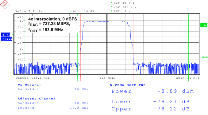
For this design example of a direct conversion transmitter, use the parameters in Table 41.
Table 41. Design Parameters
| PARAMETER | VALUE |
|---|---|
| Channel Type | 4x W-CDMA Carriers, each with 3.84 MHz bandwidth (20 MHz total bandwidth) |
| Input Data Rate | 184.32 MSPS |
| Interpolation | 4 |
| NCO Frequency | Bypassed |
| Output IF | None (Complex baseband) |
| DAC Conversion Rate (DACCLK frequency) | 737.28 MSPS |
9.2.2 Detailed Design Procedure
9.2.2.1 Direct Conversion Radio
Refer to Figure 88 for an example Direct Conversion Radio. The DAC3283 receives an interleaved complex I/Q baseband input data stream and increases the sample rate through interpolation by a factor of 2 or 4. By performing digital interpolation on the input data, undesired images of the original signal can be push out of the band of interest and more easily suppressed with analog filters.
For a Zero IF (ZIF) frequency plan, complex mixing of the baseband signal is not required. Alternatively, for a Complex IF frequency plan the input data can be pre-placed at an IF within the bandwidth limitations of the interpolation filters. In addition, complex mixing is available using the coarse mixer block to up-convert the signal. The output of both DAC channels is used to produce a Hilbert transform pair and can be expressed as:
where m(t) and mh(t) connote a Hilbert transform pair and ωc is the mixer frequency. The complex output is input to an analog quadrature modulator (AQM) such as the Texas Instruments TRF3720 for a single side-band (SSB) up conversion to RF. A passive (resistor only) interface to the AQM with an optional LC filter network is recommended. The TRF3720 includes a VCO/PLL to generate the LO frequency. Upper single-sideband upconversion is achieved at the output of the analog quadrature modulator, whose output is expressed as:
Flexibility is provided to the user by allowing for the selection of negative mixing frequency to produce a lower-sideband upconversion. Note that the process of complex mixing translates the signal frequency from 0Hz means that the analog quadrature modulator IQ imbalance produces a sideband that falls outside the signal of interest. DC offset error in DAC and AQM signal path may produce LO feed-through at the RF output which may fall in the band of interest. To suppress the LO feed-through, the DAC3283 provides a digital offset correction capability for both DAC-A and DAC-B paths. In addition phase and gain imbalances in the DAC and AQM result in a lower-sideband product. The DAC3283 offers gain and phase correction capabilities to minimize the sideband product.
The complex IF architecture has several advantages over the real IF architecture:
- Uncalibrated side-band suppression ~ 35dBc compared to 0dBc for real IF architecture.
- Direct DAC to AQM interface – no amplifiers required
- DAC 2nd Nyquist zone image is offset fDAC compared with fDAC– 2 x IF for a real IF architecture, reducing the need for filtering at the DAC output.
- Uncalibrated LO feed through for AQM is ~ 35 dBc and calibration can reduce or completely remove the LO feed through.


