ZHCS065G March 2011 – January 2024 DAC3482
PRODUCTION DATA
- 1
- 1 特性
- 2 应用
- 3 说明
- 4 Pin Configuration and Functions
-
5 Specifications
- 5.1 Absolute Maximum Ratings
- 5.2 ESD Ratings
- 5.3 Recommended Operating Conditions
- 5.4 Thermal Information
- 5.5 Electrical Characteristics – DC Specifications
- 5.6 Electrical Characteristics – Digital Specifications
- 5.7 Electrical Characteristics – AC Specifications
- 5.8 Electrical Characteristics - Phase-Locked Loop Specifications
- 5.9 Timing Requirements - Digital Specifications
- 5.10 Switching Characteristics – AC Specifications
- 5.11 Typical Characteristics
-
6 Detailed Description
- 6.1 Overview
- 6.2 Functional Block Diagram
- 6.3
Feature Description
- 6.3.1 Serial Interface
- 6.3.2 Data Interface
- 6.3.3 Input FIFO
- 6.3.4 FIFO Modes of Operation
- 6.3.5 Clocking Modes
- 6.3.6 FIR Filters
- 6.3.7 Complex Signal Mixer
- 6.3.8 Quadrature Modulation Correction (QMC)
- 6.3.9 Temperature Sensor
- 6.3.10 Data Pattern Checker
- 6.3.11 Parity Check Test
- 6.3.12 DAC3482 Alarm Monitoring
- 6.3.13 LVPECL Inputs
- 6.3.14 LVDS Inputs
- 6.3.15 Unused LVDS Port Termination
- 6.3.16 CMOS Digital Inputs
- 6.3.17 Reference Operation
- 6.3.18 DAC Transfer Function
- 6.3.19 Analog Current Outputs
- 6.4 Device Functional Modes
- 6.5 Programming
- 6.6
Register Map
- 6.6.1
Register Descriptions
- 6.6.1.1 Register Name: config0 – Address: 0x00, Default: 0x049C
- 6.6.1.2 Register Name: config1 – Address: 0x01, Default: 0x050E
- 6.6.1.3 Register Name: config2 – Address: 0x02, Default: 0x7000
- 6.6.1.4 Register Name: config3 – Address: 0x03, Default: 0xF000
- 6.6.1.5 Register Name: config4 – Address: 0x04, Default: No RESET Value (WRITE TO CLEAR)
- 6.6.1.6 Register Name: config5 – Address: 0x05, Default: Setup and Power-Up Conditions Dependent (WRITE TO CLEAR)
- 6.6.1.7 Register Name: config6 – Address: 0x06, Default: No RESET Value (READ ONLY)
- 6.6.1.8 Register Name: config7 – Address: 0x07, Default: 0xFFFF
- 6.6.1.9 Register Name: config8 – Address: 0x08, Default: 0x0000 (CAUSES AUTO-SYNC)
- 6.6.1.10 Register Name: config9 – Address: 0x09, Default: 0x8000
- 6.6.1.11 Register Name: config10 – Address: 0x0A, Default: 0x0000
- 6.6.1.12 Register Name: config11 – Address: 0x0B, Default: 0x0000
- 6.6.1.13 Register Name: config12 – Address: 0x0C, Default: 0x0400
- 6.6.1.14 Register Name: config13 – Address: 0x0D, Default: 0x0400
- 6.6.1.15 Register Name: config14 – Address: 0x0E, Default: 0x0400
- 6.6.1.16 Register Name: config15 – Address: 0x0F, Default: 0x0400
- 6.6.1.17 Register Name: config16 – Address: 0x10, Default: 0x0000 (CAUSES AUTO-SYNC)
- 6.6.1.18 Register Name: config17 – Address: 0x11, Default: 0x0000
- 6.6.1.19 Register Name: config18 – Address: 0x12, Default: 0x0000 (CAUSES AUTO-SYNC)
- 6.6.1.20 Register Name: config19 – Address: 0x13, Default: 0x0000
- 6.6.1.21 Register Name: config20 – Address: 0x14, Default: 0x0000
- 6.6.1.22 Register Name: config21 – Address: 0x15, Default: 0x0000
- 6.6.1.23 Register name: config22 – Address: 0x16, Default: 0x0000
- 6.6.1.24 Register Name: config23 – Address: 0x17, Default: 0x0000
- 6.6.1.25 Register Name: config24 – Address: 0x18, Default: NA
- 6.6.1.26 Register Name: config25 – Address: 0x19, Default: 0x0440
- 6.6.1.27 Register Name: config26 – Address: 0x1A, Default: 0x0020
- 6.6.1.28 Register Name: config27 – Address: 0x1B, Default: 0x0000
- 6.6.1.29 Register Name: config28 – Address: 0x1C, Default: 0x0000
- 6.6.1.30 Register Name: config29 – Address: 0x1D, Default: 0x0000
- 6.6.1.31 Register Name: config30 – Address: 0x1E, Default: 0x1111
- 6.6.1.32 Register Name: config31 – Address: 0x1F, Default: 0x1140
- 6.6.1.33 Register Name: config32 – Address: 0x20, Default: 0x2400
- 6.6.1.34 Register Name: config33 – Address: 0x21, Default: 0x0000
- 6.6.1.35 Register Name: config34 – Address: 0x22, Default: 0x1B1B
- 6.6.1.36 Register Name: config35 – Address: 0x23, Default: 0xFFFF
- 6.6.1.37 Register Name: config36 – Address: 0x24, Default: 0x0000
- 6.6.1.38 Register Name: config37 – Address: 0x25, Default: 0x7A7A
- 6.6.1.39 Register Name: config38 – Address: 0x26, Default: 0xB6B6
- 6.6.1.40 Register Name: config39 – Address: 0x27, Default: 0xEAEA
- 6.6.1.41 Register Name: config40 – Address: 0x28, Default: 0x4545
- 6.6.1.42 Register Name: config41 – Address: 0x29, Default: 0x1A1A
- 6.6.1.43 Register Name: config42 – Address: 0x2A, Default: 0x1616
- 6.6.1.44 Register Name: config43 – Address: 0x2B, Default: 0xAAAA
- 6.6.1.45 Register Name: config44 – Address: 0x2C, Default: 0xC6C6
- 6.6.1.46 Register Name: config45 – Address: 0x2D, Default: 0x0004
- 6.6.1.47 Register Name: config46 – Address: 0x2E, Default: 0x0000
- 6.6.1.48 Register Name: config47 – Address: 0x2F, Default: 0x0000
- 6.6.1.49 Register Name: config48 – Address: 0x30, Default: 0x0000
- 6.6.1.50 Register Name: version– Address: 0x7F, Default: 0x540C (READ ONLY)
- 6.6.1
Register Descriptions
- 7 Application and Implementation
- 8 Device and Documentation Support
- 9 Revision History
- 10Mechanical, Packaging, and Orderable Information
封装选项
机械数据 (封装 | 引脚)
散热焊盘机械数据 (封装 | 引脚)
- RKD|88
订购信息
6.3.5.2 PLL Mode
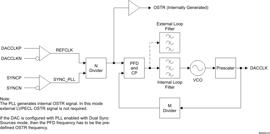
In this mode the clock at the DACCLK input functions as a reference clock source to the on-chip PLL. The on-chip PLL will then multiply this reference clock to supply a higher frequency DAC sample rate clock. Figure 6-8 shows the block diagram of the PLL circuit.
 Figure 6-8 PLL Block Diagram
The DAC3482 PLL mode is selected by setting the following:
- pll_ena bit in register config24 to 1b to route to the PLL clock path.
- pll_sleep bit in register config26 to 0b to enable the PLL and VCO.
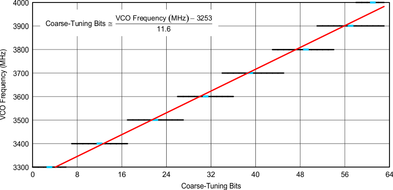
The output frequency of the VCO is designed to be the in the range from 3.3 GHz to 4.0 GHz. The prescaler value, pll_p(2:0) in register config24, should be chosen such that the product of the prescaler value and DAC sample rate clock is within the VCO range. To maintain optimal PLL loop, the coarse tune bits, pll_vco(5:0) in register config26, can adjust the center frequency of the VCO towards the product of the prescaler value and DAC sample rate clock. Figure 6-9 shows a typical relationship between coarse tune bits and VCO center frequency. For the recommended pll_vco(5:0) setting over free-air temperature, refer to Section 5.8 for details.
 Figure 6-9 Typical PLL/VCO Lock Range vs Coarse Tuning Bits
If the corresponding pll_vco(5:0) setting and the VCO frequency of interest are not in Section 5.8, TI recommends the use of the typical pll_vco(5:0) value found in Figure 6-9 along with implementation of PLL lock status check over temperature. The PLL lock status can be read back in pll_lfvolt(2:0) register of config24. If the PLL is out of range, adjust pll_vco(5:0) in config26 accordingly. The example PLL lock status and adjustment algorithm can be found in Figure 6-10.
 Figure 6-10 Example PLL Lock Status and Adjustment Algorithm
Common wireless infrastructure frequencies (614.4MHz, 737.28MHz, 983.04MHz, ...) are generated from this VCO frequency in conjunction with the pre-scaler setting as shown in Table 6-4.
| VCO FREQUENCY (MHz) | PRE-SCALE DIVIDER | DESIRED DACCLK (MHz) | pll_p(2:0) |
|---|---|---|---|
| 3932.16 | 8 | 491.52 | 111 |
| 3686.4 | 6 | 614.4 | 110 |
| 3686.4 | 5 | 737.28 | 101 |
| 3932.16 | 4 | 983.04 | 100 |
The M divider is used to determine the phase-frequency-detector (PFD) and charge-pump (CP) frequency.
| DACCLK FREQUENCY (MHz) | M DIVIDER | PDF UPDATE RATE (MHz) | pll_m(7:0) |
|---|---|---|---|
| 491.52 | 4 | 122.88 | 00000100 |
| 491.52 | 8 | 61.44 | 00001000 |
| 491.52 | 16 | 30.72 | 00010000 |
| 491.52 | 32 | 15.36 | 00100000 |
The N divider in the loop allows the PFD to operate at a lower frequency than the reference clock. Both M and N dividers can keep the PFD frequency below 155MHz for peak operation.
The overall divide ratio inside the loop is the product of the Pre-Scale and M dividers (P * M) and the following guidelines should be followed:
- The overall divide ratio range is from 24 to 480
- When the overall divide ratio is less than 120, the internal loop filter provides a stable loop
- When the overall divide ratio is greater than 120, an external loop filter or double charge pump is required for loop stability
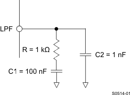
The single- and double-charge-pump current option are selected by setting pll_cp in register config24 to 01b and 11b, respectively. When using the double-charge-pump setting, an external loop filter is not required. If an external filter is required, the following filter should be connected to the LPF pin (A1 for RKD package and D12 for ZAY package):
 Figure 6-11 Recommended External Loop Filter
The PLL will generate an internal OSTR signal and does not require the external LVPECL OSTR signal. The OSTR signal is buffered from the N-divider output in the PLL block, and the frequency of the signal is the same as the PFD frequency. Therefore, using PLL with Dual Sync Sources mode requires the PFD frequency to be the pre-defined OSTR frequency listed in Section 6.3.3. This will allow the FIFO to be synced correctly by the internal OSTR.