ZHCS065G March 2011 – January 2024 DAC3482
PRODUCTION DATA
- 1
- 1 特性
- 2 应用
- 3 说明
- 4 Pin Configuration and Functions
-
5 Specifications
- 5.1 Absolute Maximum Ratings
- 5.2 ESD Ratings
- 5.3 Recommended Operating Conditions
- 5.4 Thermal Information
- 5.5 Electrical Characteristics – DC Specifications
- 5.6 Electrical Characteristics – Digital Specifications
- 5.7 Electrical Characteristics – AC Specifications
- 5.8 Electrical Characteristics - Phase-Locked Loop Specifications
- 5.9 Timing Requirements - Digital Specifications
- 5.10 Switching Characteristics – AC Specifications
- 5.11 Typical Characteristics
-
6 Detailed Description
- 6.1 Overview
- 6.2 Functional Block Diagram
- 6.3
Feature Description
- 6.3.1 Serial Interface
- 6.3.2 Data Interface
- 6.3.3 Input FIFO
- 6.3.4 FIFO Modes of Operation
- 6.3.5 Clocking Modes
- 6.3.6 FIR Filters
- 6.3.7 Complex Signal Mixer
- 6.3.8 Quadrature Modulation Correction (QMC)
- 6.3.9 Temperature Sensor
- 6.3.10 Data Pattern Checker
- 6.3.11 Parity Check Test
- 6.3.12 DAC3482 Alarm Monitoring
- 6.3.13 LVPECL Inputs
- 6.3.14 LVDS Inputs
- 6.3.15 Unused LVDS Port Termination
- 6.3.16 CMOS Digital Inputs
- 6.3.17 Reference Operation
- 6.3.18 DAC Transfer Function
- 6.3.19 Analog Current Outputs
- 6.4 Device Functional Modes
- 6.5 Programming
- 6.6
Register Map
- 6.6.1
Register Descriptions
- 6.6.1.1 Register Name: config0 – Address: 0x00, Default: 0x049C
- 6.6.1.2 Register Name: config1 – Address: 0x01, Default: 0x050E
- 6.6.1.3 Register Name: config2 – Address: 0x02, Default: 0x7000
- 6.6.1.4 Register Name: config3 – Address: 0x03, Default: 0xF000
- 6.6.1.5 Register Name: config4 – Address: 0x04, Default: No RESET Value (WRITE TO CLEAR)
- 6.6.1.6 Register Name: config5 – Address: 0x05, Default: Setup and Power-Up Conditions Dependent (WRITE TO CLEAR)
- 6.6.1.7 Register Name: config6 – Address: 0x06, Default: No RESET Value (READ ONLY)
- 6.6.1.8 Register Name: config7 – Address: 0x07, Default: 0xFFFF
- 6.6.1.9 Register Name: config8 – Address: 0x08, Default: 0x0000 (CAUSES AUTO-SYNC)
- 6.6.1.10 Register Name: config9 – Address: 0x09, Default: 0x8000
- 6.6.1.11 Register Name: config10 – Address: 0x0A, Default: 0x0000
- 6.6.1.12 Register Name: config11 – Address: 0x0B, Default: 0x0000
- 6.6.1.13 Register Name: config12 – Address: 0x0C, Default: 0x0400
- 6.6.1.14 Register Name: config13 – Address: 0x0D, Default: 0x0400
- 6.6.1.15 Register Name: config14 – Address: 0x0E, Default: 0x0400
- 6.6.1.16 Register Name: config15 – Address: 0x0F, Default: 0x0400
- 6.6.1.17 Register Name: config16 – Address: 0x10, Default: 0x0000 (CAUSES AUTO-SYNC)
- 6.6.1.18 Register Name: config17 – Address: 0x11, Default: 0x0000
- 6.6.1.19 Register Name: config18 – Address: 0x12, Default: 0x0000 (CAUSES AUTO-SYNC)
- 6.6.1.20 Register Name: config19 – Address: 0x13, Default: 0x0000
- 6.6.1.21 Register Name: config20 – Address: 0x14, Default: 0x0000
- 6.6.1.22 Register Name: config21 – Address: 0x15, Default: 0x0000
- 6.6.1.23 Register name: config22 – Address: 0x16, Default: 0x0000
- 6.6.1.24 Register Name: config23 – Address: 0x17, Default: 0x0000
- 6.6.1.25 Register Name: config24 – Address: 0x18, Default: NA
- 6.6.1.26 Register Name: config25 – Address: 0x19, Default: 0x0440
- 6.6.1.27 Register Name: config26 – Address: 0x1A, Default: 0x0020
- 6.6.1.28 Register Name: config27 – Address: 0x1B, Default: 0x0000
- 6.6.1.29 Register Name: config28 – Address: 0x1C, Default: 0x0000
- 6.6.1.30 Register Name: config29 – Address: 0x1D, Default: 0x0000
- 6.6.1.31 Register Name: config30 – Address: 0x1E, Default: 0x1111
- 6.6.1.32 Register Name: config31 – Address: 0x1F, Default: 0x1140
- 6.6.1.33 Register Name: config32 – Address: 0x20, Default: 0x2400
- 6.6.1.34 Register Name: config33 – Address: 0x21, Default: 0x0000
- 6.6.1.35 Register Name: config34 – Address: 0x22, Default: 0x1B1B
- 6.6.1.36 Register Name: config35 – Address: 0x23, Default: 0xFFFF
- 6.6.1.37 Register Name: config36 – Address: 0x24, Default: 0x0000
- 6.6.1.38 Register Name: config37 – Address: 0x25, Default: 0x7A7A
- 6.6.1.39 Register Name: config38 – Address: 0x26, Default: 0xB6B6
- 6.6.1.40 Register Name: config39 – Address: 0x27, Default: 0xEAEA
- 6.6.1.41 Register Name: config40 – Address: 0x28, Default: 0x4545
- 6.6.1.42 Register Name: config41 – Address: 0x29, Default: 0x1A1A
- 6.6.1.43 Register Name: config42 – Address: 0x2A, Default: 0x1616
- 6.6.1.44 Register Name: config43 – Address: 0x2B, Default: 0xAAAA
- 6.6.1.45 Register Name: config44 – Address: 0x2C, Default: 0xC6C6
- 6.6.1.46 Register Name: config45 – Address: 0x2D, Default: 0x0004
- 6.6.1.47 Register Name: config46 – Address: 0x2E, Default: 0x0000
- 6.6.1.48 Register Name: config47 – Address: 0x2F, Default: 0x0000
- 6.6.1.49 Register Name: config48 – Address: 0x30, Default: 0x0000
- 6.6.1.50 Register Name: version– Address: 0x7F, Default: 0x540C (READ ONLY)
- 6.6.1
Register Descriptions
- 7 Application and Implementation
- 8 Device and Documentation Support
- 9 Revision History
- 10Mechanical, Packaging, and Orderable Information
封装选项
机械数据 (封装 | 引脚)
散热焊盘机械数据 (封装 | 引脚)
- RKD|88
订购信息
6.3.3 Input FIFO
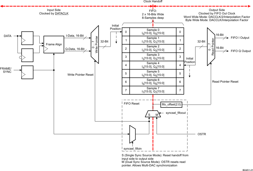
The DAC3482 includes a 2-channel, 16-bits wide, and 8-samples deep input FIFO which acts as an elastic buffer. The purpose of the FIFO is to absorb any timing variations between the input data and the internal DAC data rate clock such as the ones resulting from clock-to-data variations from the data source.
Figure 6-5 shows a simplified block diagram of the FIFO. The following sections provide brief overviews of the FIFO, device synchronization, and device clocking. For more details of the topics, refer to application report SLAA584.
 Figure 6-5 DAC3482 FIFO Block Diagram
Data is written to the device on the rising and falling edges of DATACLK. Each 32-bit wide sample (16-bit I-data and 16-bit Q-data) is written into the FIFO at the address indicated by the write pointer. Similarly, data from the FIFO is read by the FIFO Out Clock 32-bits at a time from the address indicated by the read pointer. The FIFO Out Clock is generated internally from the DACCLK signal. Its rate is equal to DACCLK/2/Interpolation for word-wide data transmission, or DACCLK/Interpolation for byte-wide data transmission. Each time a FIFO write or FIFO read is done the corresponding pointer moves to the next address.
The reset position for the FIFO read and write pointers is set by default to addresses 0 and 4 as shown in Figure 6-5. This offset gives optimal margin within the FIFO. The default read pointer location can be set to another value using fifo_offset(2:0) in register config9 (address 4 by default). Under normal conditions data is written-to and read-from the FIFO at the same rate and consequently the write and read pointer gap remains constant. If the FIFO write and read rates are different, the corresponding pointers will be cycling at different speeds which could result in pointer collision. Under this condition the FIFO attempts to read and write data from the same address at the same time which will result in errors and thus must be avoided.
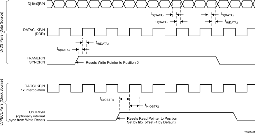
The write pointer sync source is selected by syncsel_fifoin(3:0) in register config32. In most applications either FRAME or SYNC is used to reset the write pointer. Unlike DATA, the sync signal is latched only on the rising edges of DATACLK. A rising edge on the sync signal source causes the pointer to return to its original position.
Similarly, the read pointer sync source is selected by syncsel_fifoout(3:0). The write pointer sync source can be set to reset the read pointer as well. In this case, the FIFO Out clock recaptures the write pointer sync signal to reset the read pointer. This clock domain transfer (DATACLK to FIFO Out Clock) results in phase ambiguity of the reset signal, and will create latency variation based on the capture edge of the FIFO Out Clock. Since the reset signal also synchronizes the clock divider circuit for the FIFO Out clock generation, the latency variation also includes the capture edge of the DACCLK cycle in the clock divider stage. Ultimately, the variation in capture edge of both the FIFO Out clock and the DACCLK limits the precise control of the output timing latency. The full latency control of the DAC will be difficult and is not recommended in this setup.
For full latency control of the DAC, refer to Section 6.3.4.1 of the datasheet.
To alleviate this, the device offers the alternative of resetting the FIFO read pointer independently of the write pointer by using the OSTR signal. The OSTR signal is sampled by DACCLK and must satisfy the timing requirements in the specifications table. To minimize the skew, it is recommended to use the same clock distribution device such as Texas Instruments CDCE62005 or LMK0480x family to provide the DACCLK and OSTR signals to all the DAC3482 devices in the system. Swapping the polarity of the DACCLK outputs with respect to the OSTR ones establishes proper phase relationship.
The FIFO pointers reset procedure can be done periodically or only once during initialization as the pointers automatically return to the initial position when the FIFO has been filled. To reset the FIFO periodically, the signals to sync the FIFO read and write pointer can repeat at multiples of 8 FIFO samples when the data interface is byte-wide format. When the data interface is word-wide format, the signal to sync the FIFO read and write pointer can repeat at multiples of 16 FIFO samples.
The frequency limitation for FRAME and SYNC signals are the following:
where n = 1, 2, … can repeat multiples of 8 FIFO samples for Byte-Wide Mode
where n = 1, 2, … can repeat multiples of 16 FIFO samples for Word-Wide Mode
The frequency limitation for the OSTR signal is the following:
where n = 1, 2, … can repeat multiples of 8 FIFO samples for Byte-Wide Mode
where n = 1, 2, … can repeat multiples of 16 FIFO samples for World-Wide Mode
The frequencies above are at maximum when n = 1. This is when the FRAME, SYNC, or OSTR have a rising edge transition every 8 or 16 FIFO samples. The occurrence can be made less frequent by setting n > 1, for example, every n × 8 or n × 16 FIFO samples.
 Figure 6-6 FIFO Write and Read Descriptions (Example shown with Word-Wide Mode)