ZHCS065G March 2011 – January 2024 DAC3482
PRODUCTION DATA
- 1
- 1 特性
- 2 应用
- 3 说明
- 4 Pin Configuration and Functions
-
5 Specifications
- 5.1 Absolute Maximum Ratings
- 5.2 ESD Ratings
- 5.3 Recommended Operating Conditions
- 5.4 Thermal Information
- 5.5 Electrical Characteristics – DC Specifications
- 5.6 Electrical Characteristics – Digital Specifications
- 5.7 Electrical Characteristics – AC Specifications
- 5.8 Electrical Characteristics - Phase-Locked Loop Specifications
- 5.9 Timing Requirements - Digital Specifications
- 5.10 Switching Characteristics – AC Specifications
- 5.11 Typical Characteristics
-
6 Detailed Description
- 6.1 Overview
- 6.2 Functional Block Diagram
- 6.3
Feature Description
- 6.3.1 Serial Interface
- 6.3.2 Data Interface
- 6.3.3 Input FIFO
- 6.3.4 FIFO Modes of Operation
- 6.3.5 Clocking Modes
- 6.3.6 FIR Filters
- 6.3.7 Complex Signal Mixer
- 6.3.8 Quadrature Modulation Correction (QMC)
- 6.3.9 Temperature Sensor
- 6.3.10 Data Pattern Checker
- 6.3.11 Parity Check Test
- 6.3.12 DAC3482 Alarm Monitoring
- 6.3.13 LVPECL Inputs
- 6.3.14 LVDS Inputs
- 6.3.15 Unused LVDS Port Termination
- 6.3.16 CMOS Digital Inputs
- 6.3.17 Reference Operation
- 6.3.18 DAC Transfer Function
- 6.3.19 Analog Current Outputs
- 6.4 Device Functional Modes
- 6.5 Programming
- 6.6
Register Map
- 6.6.1
Register Descriptions
- 6.6.1.1 Register Name: config0 – Address: 0x00, Default: 0x049C
- 6.6.1.2 Register Name: config1 – Address: 0x01, Default: 0x050E
- 6.6.1.3 Register Name: config2 – Address: 0x02, Default: 0x7000
- 6.6.1.4 Register Name: config3 – Address: 0x03, Default: 0xF000
- 6.6.1.5 Register Name: config4 – Address: 0x04, Default: No RESET Value (WRITE TO CLEAR)
- 6.6.1.6 Register Name: config5 – Address: 0x05, Default: Setup and Power-Up Conditions Dependent (WRITE TO CLEAR)
- 6.6.1.7 Register Name: config6 – Address: 0x06, Default: No RESET Value (READ ONLY)
- 6.6.1.8 Register Name: config7 – Address: 0x07, Default: 0xFFFF
- 6.6.1.9 Register Name: config8 – Address: 0x08, Default: 0x0000 (CAUSES AUTO-SYNC)
- 6.6.1.10 Register Name: config9 – Address: 0x09, Default: 0x8000
- 6.6.1.11 Register Name: config10 – Address: 0x0A, Default: 0x0000
- 6.6.1.12 Register Name: config11 – Address: 0x0B, Default: 0x0000
- 6.6.1.13 Register Name: config12 – Address: 0x0C, Default: 0x0400
- 6.6.1.14 Register Name: config13 – Address: 0x0D, Default: 0x0400
- 6.6.1.15 Register Name: config14 – Address: 0x0E, Default: 0x0400
- 6.6.1.16 Register Name: config15 – Address: 0x0F, Default: 0x0400
- 6.6.1.17 Register Name: config16 – Address: 0x10, Default: 0x0000 (CAUSES AUTO-SYNC)
- 6.6.1.18 Register Name: config17 – Address: 0x11, Default: 0x0000
- 6.6.1.19 Register Name: config18 – Address: 0x12, Default: 0x0000 (CAUSES AUTO-SYNC)
- 6.6.1.20 Register Name: config19 – Address: 0x13, Default: 0x0000
- 6.6.1.21 Register Name: config20 – Address: 0x14, Default: 0x0000
- 6.6.1.22 Register Name: config21 – Address: 0x15, Default: 0x0000
- 6.6.1.23 Register name: config22 – Address: 0x16, Default: 0x0000
- 6.6.1.24 Register Name: config23 – Address: 0x17, Default: 0x0000
- 6.6.1.25 Register Name: config24 – Address: 0x18, Default: NA
- 6.6.1.26 Register Name: config25 – Address: 0x19, Default: 0x0440
- 6.6.1.27 Register Name: config26 – Address: 0x1A, Default: 0x0020
- 6.6.1.28 Register Name: config27 – Address: 0x1B, Default: 0x0000
- 6.6.1.29 Register Name: config28 – Address: 0x1C, Default: 0x0000
- 6.6.1.30 Register Name: config29 – Address: 0x1D, Default: 0x0000
- 6.6.1.31 Register Name: config30 – Address: 0x1E, Default: 0x1111
- 6.6.1.32 Register Name: config31 – Address: 0x1F, Default: 0x1140
- 6.6.1.33 Register Name: config32 – Address: 0x20, Default: 0x2400
- 6.6.1.34 Register Name: config33 – Address: 0x21, Default: 0x0000
- 6.6.1.35 Register Name: config34 – Address: 0x22, Default: 0x1B1B
- 6.6.1.36 Register Name: config35 – Address: 0x23, Default: 0xFFFF
- 6.6.1.37 Register Name: config36 – Address: 0x24, Default: 0x0000
- 6.6.1.38 Register Name: config37 – Address: 0x25, Default: 0x7A7A
- 6.6.1.39 Register Name: config38 – Address: 0x26, Default: 0xB6B6
- 6.6.1.40 Register Name: config39 – Address: 0x27, Default: 0xEAEA
- 6.6.1.41 Register Name: config40 – Address: 0x28, Default: 0x4545
- 6.6.1.42 Register Name: config41 – Address: 0x29, Default: 0x1A1A
- 6.6.1.43 Register Name: config42 – Address: 0x2A, Default: 0x1616
- 6.6.1.44 Register Name: config43 – Address: 0x2B, Default: 0xAAAA
- 6.6.1.45 Register Name: config44 – Address: 0x2C, Default: 0xC6C6
- 6.6.1.46 Register Name: config45 – Address: 0x2D, Default: 0x0004
- 6.6.1.47 Register Name: config46 – Address: 0x2E, Default: 0x0000
- 6.6.1.48 Register Name: config47 – Address: 0x2F, Default: 0x0000
- 6.6.1.49 Register Name: config48 – Address: 0x30, Default: 0x0000
- 6.6.1.50 Register Name: version– Address: 0x7F, Default: 0x540C (READ ONLY)
- 6.6.1
Register Descriptions
- 7 Application and Implementation
- 8 Device and Documentation Support
- 9 Revision History
- 10Mechanical, Packaging, and Orderable Information
封装选项
机械数据 (封装 | 引脚)
散热焊盘机械数据 (封装 | 引脚)
- RKD|88
订购信息
6.3.1 Serial Interface
The serial port of the DAC3482 is a flexible serial interface which communicates with industry standard microprocessors and microcontrollers. The interface provides read/write access to all registers used to define the operating modes of DAC3482. It is compatible with most synchronous transfer formats and can be configured as a 3 or 4-pin interface by sif4_ena in register config2. In both configurations, SCLK is the serial interface input clock and SDENB is serial interface enable. For 3-pin configuration, SDIO is a bidirectional pin for both data in and data out. For 4 pin configuration, SDIO is data in only and SDO is data out only. Data is input into the device with the rising edge of SCLK. Data is output from the device on the falling edge of SCLK.
Each read/write operation is framed by signal SDENB (Serial Data Enable Bar) asserted low. The first frame byte is the instruction cycle which identifies the following data transfer cycle as read or write as well as the 7-bit address to be accessed. Table 6-1 below indicates the function of each bit in the instruction cycle and is followed by a detailed description of each bit. The data transfer cycle consists of two bytes.
| Bit | 7 (MSB) | 6 | 5 | 4 | 3 | 2 | 1 | 0 (LSB) |
| Description | R/W | A6 | A5 | A4 | A3 | A2 | A1 | A0 |
| R/W | Identifies the following data transfer cycle as a read or write operation. A high indicates a read operation from DAC3482 and a low indicates a write operation to DAC3482. |
| [A6 : A0] | Identifies the address of the register to be accessed during the read or write operation. |
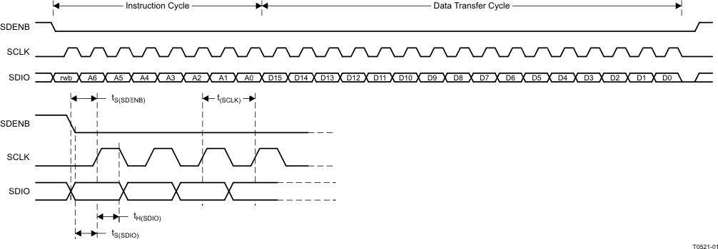
Figure 6-1 shows the serial interface timing diagram for a DAC3482 write operation. SCLK is the serial interface clock input to DAC3482. Serial data enable SDENB is an active low input to DAC3482. SDIO is serial data in. Input data to DAC3482 is clocked on the rising edges of SCLK.
 Figure 6-1 Serial Interface Write Timing Diagram
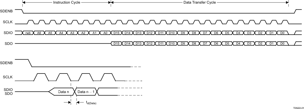
Figure 6-2 shows the serial interface timing diagram for a DAC3482 read operation. SCLK is the serial interface clock input to DAC3482. Serial data enable SDENB is an active low input to DAC3482. SDIO is serial data in during the instruction cycle. In 3-pin configuration, SDIO is data out from the DAC3482 during the data transfer cycle, while SDO is in a high-impedance state. In 4-pin configuration, SDO is data out from the DAC3482 during the data transfer cycle. At the end of the data transfer, SDIO and SDO will output low on the final falling edge of SCLK until the rising edge of SDENB when they will 3-state.
 Figure 6-2 Serial Interface Read Timing Diagram