ZHCS072E March   2011  – November 2015 DAC3484

PRODUCTION DATA.  

  1. 特性
  2. 应用范围
  3. 说明
  4. 修订历史记录
  5. Pin Configuration and Functions
  6. Specifications
    1. 6.1  Absolute Maximum Ratings
    2. 6.2  ESD Ratings
    3. 6.3  Recommended Operating Conditions
    4. 6.4  Thermal InformationZAY package information to Thermal InformationTJ row from top of thermal table
    5. 6.5  Electrical Characteristics - DC Specifications
    6. 6.6  Electrical Characteristics - Digital Specifications
    7. 6.7  Electrical Characteristics - AC Specifications
    8. 6.8  Timing Requirements - Digital Specifications
    9. 6.9  Switching Characteristics - AC Specifications
    10. 6.10 Typical Characteristics
  7. Detailed Description
    1. 7.1 Overview
    2. 7.2 Functional Block Diagram
    3. 7.3 Feature Description
      1. 7.3.1  Serial Interface
      2. 7.3.2  Data Interface
        1. 7.3.2.1 Word-Wide Format
        2. 7.3.2.2 Byte-Wide Format
      3. 7.3.3  Input FIFO
      4. 7.3.4  FIFO Modes of Operation
        1. 7.3.4.1 Dual Sync Sources Mode
        2. 7.3.4.2 Single Sync Source Mode
        3. 7.3.4.3 Bypass Mode
      5. 7.3.5  Clocking Modes
        1. 7.3.5.1 PLL Bypass Mode
        2. 7.3.5.2 PLL Mode
      6. 7.3.6  FIR Filters
      7. 7.3.7  Complex Signal Mixer
        1. 7.3.7.1 Full Complex Mixer
        2. 7.3.7.2 Coarse Complex Mixer
        3. 7.3.7.3 Mixer Gain
        4. 7.3.7.4 Real Channel Upconversion
      8. 7.3.8  Quadrature Modulation Correction (QMC)
        1. 7.3.8.1 Gain and Phase Correction
        2. 7.3.8.2 Offset Correction
        3. 7.3.8.3 Group Delay Correction
      9. 7.3.9  Temperature Sensor
      10. 7.3.10 Data Pattern Checker
      11. 7.3.11 Parity Check Test
        1. 7.3.11.1 Word-by-Word Parity
        2. 7.3.11.2 Block Parity
      12. 7.3.12 DAC3484 Alarm Monitoring
      13. 7.3.13 LVPECL Inputs
      14. 7.3.14 LVDS Inputs
      15. 7.3.15 Unused LVDS Port Termination
      16. 7.3.16 CMOS Digital Inputs
      17. 7.3.17 Reference Operation
      18. 7.3.18 DAC Transfer Function
      19. 7.3.19 Analog Current Outputs
    4. 7.4 Device Functional Modes
      1. 7.4.1 Multi-Device Synchronization
        1. 7.4.1.1 Multi-Device Synchronization: PLL Bypassed with Dual Sync Sources Mode
        2. 7.4.1.2 Multi-Device Synchronization: PLL Enabled with Dual Sync Sources Mode
        3. 7.4.1.3 Multi-Device Operation: Single Sync Source Mode
    5. 7.5 Programming
      1. 7.5.1 Power-Up Sequence
      2. 7.5.2 Example Start-Up Routine
        1. 7.5.2.1 Device Configuration
        2. 7.5.2.2 PLL Configuration
        3. 7.5.2.3 NCO Configuration
        4. 7.5.2.4 Example Start-Up Sequence
    6. 7.6 Register Map
      1. 7.6.1 Register Descriptions
  8. Application and Implementation
    1. 8.1 Application Information
    2. 8.2 Typical Applications
      1. 8.2.1 IF Based LTE Transmitter
        1. 8.2.1.1 Design Requirements
        2. 8.2.1.2 Detailed Design Procedure
          1. 8.2.1.2.1 Data Input Rate
          2. 8.2.1.2.2 Interpolation
          3. 8.2.1.2.3 LO Feedthrough and Sideband Correction
        3. 8.2.1.3 Application Curves
      2. 8.2.2 Direct Upconversion (Zero IF) LTE Transmitter
        1. 8.2.2.1 Design Requirements
        2. 8.2.2.2 Detailed Design Procedure
          1. 8.2.2.2.1 Data Input Rate
          2. 8.2.2.2.2 Interpolation
          3. 8.2.2.2.3 LO Feedthrough and Sideband Correction
        3. 8.2.2.3 Application Curves
  9. Power Supply Recommendations
  10. 10Layout
    1. 10.1 Layout Guidelines
      1. 10.1.1 Assembly
    2. 10.2 Layout Examples
  11. 11器件和文档支持
    1. 11.1 器件支持
      1. 11.1.1 Third-Party Products Disclaimer
      2. 11.1.2 器件命名规则
        1. 11.1.2.1 技术参数定义
    2. 11.2 文档支持
      1. 11.2.1 相关文档 
    3. 11.3 社区资源
    4. 11.4 商标
    5. 11.5 静电放电警告
    6. 11.6 Glossary
  12. 12机械、封装和可订购信息

封装选项

机械数据 (封装 | 引脚)
散热焊盘机械数据 (封装 | 引脚)
订购信息

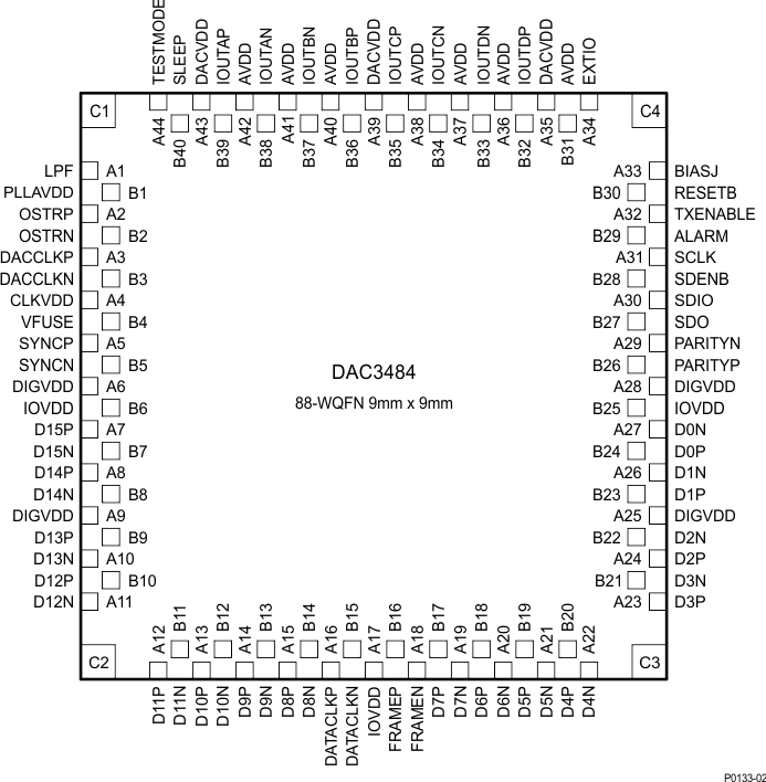
5 Pin Configuration and Functions

RKD Package
88-Pin WQFN
Top View
DAC3484 P0133-02_LAS749.gif

Pin Functions - WQFN

PIN I/O DESCRIPTION
NAME NO.
AVDD A36, A37, A38, A40, A41, A42, B31 I Analog supply voltage. (3.3 V)
ALARM B29 O CMOS output for ALARM condition. The ALARM output functionality is defined through the config7 register. Default polarity is active high, but can be changed to active low via config0 alarm_out_pol control bit.
BIASJ A33 O Full-scale output current bias. For 30-mA full-scale output current, connect 1.28 kΩ to ground. Change the full-scale output current through coarse_dac(3:0) in config3, bit<15:12>
CLKVDD A4 I Internal clock buffer supply voltage. (1.2 V)
It is recommended to isolate this supply from DIGVDD and DACVDD.
D[15..0]P A7, A8, B9, B10, A12, A13, A14, A15, B17, B18, B19, B20, A23, A24, B23, B24 I LVDS positive input data bits 0 through 15. Internal 100-Ω termination resistor. Data format relative to DATACLKP/N clock is Double Data Rate (DDR).
D15P is most significant data bit (MSB)
D0P is least significant data bit (LSB)
The order of the bus can be reversed via config2 revbus bit.
D[15..0]N B7, B8, A10, A11, B11, B12, B13, B14, A19, A20, A21, A22, B21, B22, A26, A27 I LVDS negative input data bits 0 through 15. (See D[15:0]P description above)
DACCLKP A3 I Positive external LVPECL clock input for DAC core with a self-bias.
DACCLKN B3 I Complementary external LVPECL clock input for DAC core. (see the DACCLKP description)
DACVDD A35, A39, A43 I DAC core supply voltage. (1.2 V). It is recommended to isolate this supply from CLKVDD and DIGVDD.
DATACLKP A16 I LVDS positive input data clock. Internal 100 Ω termination resistor. Input data D[15:0]P/N is latched on both edges of DATACLKP/N (Double Data Rate).
DATACLKN B15 I LVDS negative input data clock. (See DATACLKP description)
DIGVDD A6, A9, A25, A28 I Digital supply voltage. (1.2 V). It is recommended to isolate this supply from CLKVDD and DACVDD.
EXTIO A34 I/O Used as external reference input when internal reference is disabled through config27 extref_ena = 1b. Used as internal reference output when config27 extref_ena = 0b (default). Requires a 0.1-µF decoupling capacitor to AGND when used as reference output.
FRAMEP B16 I LVDS frame indicator positive input. Internal 100-Ω termination resistor.
The main functions of this input are to reset the FIFO pointer or to be used as a syncing source. These two functions are captured with the rising edge of DATACLKP/N. The signal captured by the falling edge of DATACLKP/N can be used as a block parity bit. The FRAMEP/N signal should be edge-aligned with D[15:0]P/N.
Additionally it is used to indicate the beginning of the frame.
FRAMEN A18 I LVDS frame indicator negative input. (See the FRAMEP description)
GND C1, C2, C3, C4, Thermal Pad I These pins are ground for all supplies.
IOUTAP B39 O A-Channel DAC current output. Connect directly to ground if unused.
IOUTAN B38 O A-Channel DAC complementary current output. Connect directly to ground if unused.
IOUTBP B36 O B-Channel DAC current output. Connect directly to ground if unused.
IOUTBN B37 O B-Channel DAC complementary current output. Connect directly to ground if unused.
IOUTCP B35 O C-Channel DAC current output. Connect directly to ground if unused.
IOUTCN B34 O C-Channel DAC complementary current output. Connect directly to ground if unused.
IOUTDP B32 O D-Channel DAC current output. Connect directly to ground if unused.
IOUTDN B33 O D-Channel DAC complementary current output. Connect directly to ground if unused.
IOVDD B6, A17, B25 I Supply voltage for all digital I/O. (3.3 V)
LPF A1 I/O PLL loop filter connection. If not using the clock multiplying PLL, the LPF pin can be left unconnected.
OSTRP A2 I LVPECL output strobe positive input. This positive/negative pair is captured with the rising edge of DACCLKP/N. It is used for multiple DAC synchronization. If unused it can be left unconnected.
OSTRN B2 I LVPECL output strobe negative input. (See the OSTRP description)
PARITYP B26 I Optional LVDS positive input parity bit. The PARITYP/N LVDS pair has an internal 100 Ω termination resistor. If unused it can be left unconnected.
PARITYN A29 I Optional LVDS negative input parity bit.
PLLAVDD B1 I PLL analog supply voltage. (3.3 V)
SCLK A31 I Serial interface clock. Internal pull-down.
SDENB B28 I Active low serial data enable, always an input to the DAC3484. Internal pull-up.
SDIO A30 I/O Serial interface data. Bi-directional in 3-pin mode (default) and uni-directional 4-pin mode. Internal pull-down.
SDO B27 O Uni-directional serial interface data in 4-pin mode. The SDO pin is tri-stated in 3-pin interface mode (default).
SLEEP B40 I Active high asynchronous hardware power-down input. Internal pull-down. If SLEEP pin is set to logic HIGH before and during device power-up and initialization, the fuse_sleep bit in register 0x1B, bit 11 must be written after register 0x23 during device initialization register setup.
SYNCP A5 I Optional LVDS SYNC positive input. The SYNCP/N LVDS pair has an internal 100-Ω termination resistor. If unused it can be left unconnected.
SYNCN B5 I Optional LVDS SYNC negative input.
RESETB B30 I Active low input for chip RESET, which resets all the programming registers to their default state. Internal pull-up.
TXENABLE A32 I Transmit enable active high input. Internal pull-down.
To enable analog output data transmission, set sif_txenable in register config3 to 1b or pull CMOS TXENABLE pin to high.
To disable analog output, set sif_txenable to 0b and pull CMOS TXENABLE pin to low. The DAC output is forced to midscale.
TESTMODE A44 I This pin is used for factory testing. Internal pull-down. Leave unconnected for normal operation.
VFUSE B4 I Digital supply voltage. This supply pin is also used for factory fuse programming. Connect to DACVDD for normal operation.
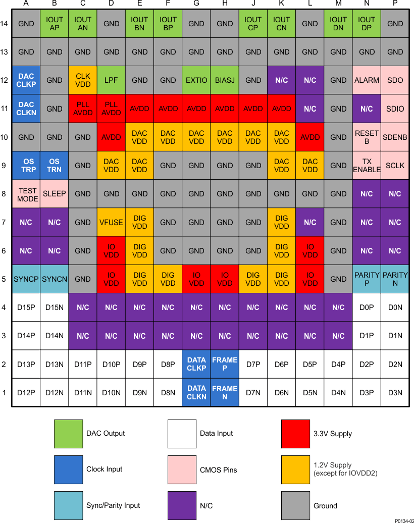
ZAY Package
196-Pin NFBGA
Top View
DAC3484 P0134-02_LAS749.gif

Pin Functions - NFBGA

PIN I/O DESCRIPTION
NAME NO.
AVDD D10, E11, F11, G11, H11, J11, K11, L10 I Analog supply voltage. (3.3 V)
ALARM N12 O CMOS output for ALARM condition. The ALARM output functionality is defined through the config7 register. Default polarity is active low, but can be changed to active high via config0 alarm_out_pol control bit.
BIASJ H12 O Full-scale output current bias. For 30-mA full-scale output current, connect 1.28 kΩ to ground. Change the full-scale output current through coarse_dac(3:0) in config3, bit<15:12>
CLKVDD C12 I Internal clock buffer supply voltage. (1.2 V)
It is recommended to isolate this supply from DIGVDD and DACVDD.
D[15..0]P N4, N3, N2, N1, M2, L2, K2, J2, F2, E2, D2, C2, A1, A2, A3, A4 I LVDS positive input data bits 0 through 15. Internal 100-Ω termination resistor. Data format relative to DATACLKP/N clock is Double Data Rate (DDR).
D15P is most significant data bit (MSB)
D0P is least significant data bit (LSB)
The order of the bus can be reversed via config2 revbus bit.
D[15..0]N P4, P3, P2, P1, M1, L1, K1, J1, F1, E1, D1, C1, B1, B2, B3, B4 I LVDS negative input data bits 0 through 15. (See D[15:0]P description above)
DACCLKP A12 I Positive external LVPECL clock input for DAC core with a self-bias.
DACCLKN A11 I Complementary external LVPECL clock input for DAC core. (see the DACCLKP description)
DACVDD D9, E9, E10, F10, G10, H10, J10, K9, K10, L9 I DAC core supply voltage. (1.2 V). It is recommended to isolate this supply from CLKVDD and DIGVDD.
DATACLKP G2 I LVDS positive input data clock. Internal 100-Ω termination resistor. Input data D[15:0]P/N is latched on both edges of DATACLKP/N (Double Data Rate).
DATACLKN G1 I LVDS negative input data clock. (See DATACLKP description)
DIGVDD E5, E6, E7, F5, J5, K5, K6, K7 I Digital supply voltage. (1.2 V). It is recommended to isolate this supply from CLKVDD and DACVDD.
EXTIO G12 I/O Used as external reference input when internal reference is disabled through config27 extref_ena = 1b. Used as internal reference output when config27 extref_ena = 0b (default). Requires a 0.1-µF decoupling capacitor to AGND when used as reference output.
FRAMEP H2 I LVDS frame indicator positive input. Internal 100-Ω termination resistor.
The main functions of this input are to reset the FIFO pointer or to be used as a syncing source. These two functions are captured with the rising edge of DATACLKP/N. The signal captured by the falling edge of DATACLKP/N can be used as a block parity bit. The FRAMEP/N signal should be edge-aligned with D[15:0]P/N.
Additionally it is used to indicate the beginning of the frame.
FRAMEN H1 I LVDS frame indicator negative input. (See the FRAMEP description)
GND A10, A13, A14, B10, B11, B12, B13, C5, C6, C7, C8, C9, C10, C13, D8, D13, D14, E8, E12, E13, F6, F7, F8, F9, F12, F13, G6, G7, G8, G9, G13, G14, H6, H7, H8, H9, H13, H14, J6, J7, J8, J9, J12, J13, K8, K13, L8, L13, L14, M5, M6, M7, M8, M9, M10, M11, M12, M13, N13, P13, P14 I These pins are ground for all supplies.
IOUTAP B14 O A-Channel DAC current output. Connect directly to ground if unused.
IOUTAN C14 O A-Channel DAC complementary current output. Connect directly to ground if unused.
IOUTBP F14 O B-Channel DAC current output. Connect directly to ground if unused.
IOUTBN E14 O B-Channel DAC complementary current output. Connect directly to ground if unused.
IOUTCP J14 O C-Channel DAC current output. Connect directly to ground if unused.
IOUTCN K14 O C-Channel DAC complementary current output. Connect directly to ground if unused.
IOUTDP N14 O D-Channel DAC current output. Connect directly to ground if unused.
IOUTDN M14 O D-Channel DAC complementary current output. Connect directly to ground if unused.
IOVDD D5, D6, G5, H5, L5, L6 I Supply voltage for all digital I/O. (3.3 V)
LPF D12 I PLL loop filter connection. If not using the clock multiplying PLL, the LPF pin can be left unconnected.
OSTRP A9 I LVPECL output strobe positive input. This positive/negative pair is captured with the rising edge of DACCLKP/N. It is used for multiple DAC synchronization. If unused it can be left unconnected.
OSTRN B9 I LVPECL output strobe negative input. (See the OSTRP description)
PARITYP N5 I Optional LVDS positive input parity bit. The PARITYP/N LVDS pair has an internal 100-Ω termination resistor. If unused it can be left unconnected.
PARITYN P5 I Optional LVDS negative input parity bit.
PLLAVDD C11, D11 I PLL analog supply voltage. (3.3 V)
SCLK P9 I Serial interface clock. Internal pull-down.
SDENB P10 I Active low serial data enable, always an input to the DAC3484. Internal pull-up.
SDIO P11 I/O Serial interface data. Bi-directional in 3-pin mode (default) and 4-pin mode. Internal pull-down.
SDO P12 O Uni-directional serial interface data in 4-pin mode. The SDO pin is three-stated in 3-pin interface mode (default).
SLEEP B8 I Active high asynchronous hardware power-down input. Internal pull-down. If SLEEP pin is set to logic HIGH before and during device power-up and initialization, the fuse_sleep bit in register 0x1B, bit 11 must be written after register 0x23 during device initialization register setup.
SYNCP A5 I Optional LVDS SYNC positive input. The SYNCP/N LVDS pair has an internal 100-Ω termination resistor. If unused it can be left unconnected.
SYNCN B5 I LVDS SYNC negative input.
RESETB N10 I Active low input for chip RESET, which resets all the programming registers to their default state. Internal pull-up.
TXENABLE N9 I Transmit enable active high input. Internal pull-down.
To enable analog output data transmission, set sif_txenable in register config3 to 1b or pull CMOS TXENABLE pin to high.
To disable analog output, set sif_txenable to 0b and pull CMOS TXENABLE pin to low. The DAC output is forced to midscale.
TESTMODE A8 O This pin is used for factory testing. Internal pull-down. Leave unconnected for normal operation.
VFUSE D7 I Digital supply voltage. This supply pin is also used for factory fuse programming. Connect to DACVDD for normal operation.