ZHCS964E February 2012 – September 2015 DAC34SH84
PRODUCTION DATA.
- 1 特性
- 2 应用范围
- 3 说明
- 4 修订历史记录
- 5 Pin Configuration and Functions
-
6 Specifications
- 6.1 Absolute Maximum Ratings
- 6.2 ESD Ratings
- 6.3 Recommended Operating Conditions
- 6.4 Thermal Information
- 6.5 Electrical Characteristics - DC Specifications
- 6.6 Electrical Characteristics - Digital Specifications
- 6.7 Electrical Characteristics - AC Specifications
- 6.8 Timing Requirements - Digital Specifications
- 6.9 Switching Characteristics - AC Specifications
- 6.10 Typical Characteristics
-
7 Detailed Description
- 7.1 Overview
- 7.2 Functional Block Diagram
- 7.3
Feature Description
- 7.3.1 Serial Interface
- 7.3.2 Data Interface
- 7.3.3 Data Format
- 7.3.4 Input FIFO
- 7.3.5 FIFO Modes of Operation
- 7.3.6 Clocking Modes
- 7.3.7 FIR Filters
- 7.3.8 Complex Signal Mixer
- 7.3.9 Quadrature Modulation Correction (QMC)
- 7.3.10 Temperature Sensor
- 7.3.11 Data Pattern Checker
- 7.3.12 Parity Check Test
- 7.3.13 DAC34SH84 Alarm Monitoring
- 7.3.14 LVPECL Inputs
- 7.3.15 LVDS Inputs
- 7.3.16 CMOS Digital Inputs
- 7.3.17 Reference Operation
- 7.3.18 DAC Transfer Function
- 7.3.19 Analog Current Outputs
- 7.4 Device Functional Modes
- 7.5 Programming
- 7.6 Register Map
- 8 Application and Implementation
- 9 Power Supply Recommendations
- 10Layout
- 11器件和文档支持
- 12机械、封装和可订购信息
9 Power Supply Recommendations
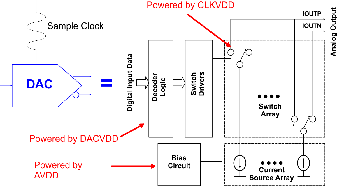
As shown in Figure 96, the DAC34SH84 device has various power rails and has three primary voltages of 1.3 V, 1.35 V, and 3.3 V. Some of the DAC power rails such as CLKVDD and AVDD are more noise sensitive than other rails because they are mainly powering the switch drivers for the current switch array and the current bias circuits, respectively. These circuits are the main analog DAC core. Any power supply noises such as switching power supply ripple may be modulated directly onto the signal of interest. These two power rails should be powered by low noise power supplies such as LDO. Powering the rail directly with switching power supplies is not recommended for these two rails.
 Figure 96. Interpolation Filters, NCOs, and QMC Blocks Powered by DIGVDD
With the DAC34SH84 being a mixed signal device, the device contains circuits that bridges the digital section and the analog section. The DACVDD powers these sections. System designer can design this rail in secondary priority. Powering the rail with LDO is recommended. Unless system designer pays special care to supply filtering and power supply routing/placement, powering the rail directly with switching power supplies is not recommended for this rail.
Since digital circuits have more inherent noise immunity than analog circuits, the power supply noise requirements for DIGVDD of the digital section of the device may be relaxed and placed at a lower priority. Depending on the spur level requirement, routing and placement of the power supply, power the rail directly with switching power supplies can be possible. With the digital logics running, the DIGVDD rail may draw significant current. If the power supply traces and filtering network have significant DC resistance loss (for example, DCR), then the final supply voltage seen by the DIGVDD rail may not be sufficient to meet the minimum power supply level. For instance, with 450 mA of DIGVDD current and about 0.1 Ω of DCR from the ferrite bead, the final supply voltage at the DIGVDD pins may be 1.3 V – 0.045 V = 1.255 V. This is fairly close to the minimum supply voltage range of 1.25 V. System designer may need to elevate the power supply voltage according to the DCR level or design a feedback network for the power supply to account for associated voltage drop. To ensure power supply accuracy and to account for power supply filter network loss at operating conditions, the use of the ATEST function in register config27 to check the internal power supply nodes is recommended.
The table below is a summary of the various power supply nodes of the DAC. Care should be taken to keep clean power supplies routing away from noisy digital supplies. It is recommended to use at least two power layers. Power supplies for digital circuits tend to have more switching activities and are typically noisier, and system designer should avoid sharing the digital power rail (for example, power supplies for FPGA or DIGVDD of DAC34SH84) with the analog power rail (for example, CLKVDD and AVDD of DAC34SH84). Avoid placing noisy supplies and clean supplies on adjacent board layers and use a ground layer between these two supplies if possible. All supply pins should be decoupled as close to the pins as possible by using small value capacitors, with larger bulk capacitors placed further away and near the power supply source.
Table 66. Power Rails
| POWER RAILS |
TYPICAL VOLTAGE |
NOISE SENSITIVITY |
RECOMMENDATIONS | POWER SUPPLY DESIGN PRIORITY |
|---|---|---|---|---|
| CLKVDD | 1.35 V | High | Provide clean supply to the rail. Avoid spurious noise or coupling from other supplies | High |
| AVDD | 3.3 V | High | Provide clean supply to the rail. Avoid spurious noise or coupling from other supplies | High |
| DACVDD | 1.35 V | Medium | Provide clean supply to the rail. Avoid spurious noise or coupling from other supplies | Medium |
| DIGVDD | 1.3 V | Low | Keep Away from other noise sensitive nodes in placement and routing. | Low |