ZHCSGG0B February 2017 – July 2017 DAC38RF86 , DAC38RF87 , DAC38RF96 , DAC38RF97
PRODUCTION DATA.
- 1 特性
- 2 应用
- 3 说明
- 4 修订历史记录
- 5 Device Comparison Table
- 6 Pin Configuration and Functions
-
7 Specifications
- 7.1 Absolute Maximum Ratings
- 7.2 ESD Ratings
- 7.3 Recommended Operating Conditions
- 7.4 Thermal Information
- 7.5 Electrical Characteristics - DC Specifications
- 7.6 Electrical Characteristics - Digital Specifications
- 7.7 Electrical Characteristics - AC Specifications
- 7.8 PLL/VCO Electrical Characteristics
- 7.9 Timing Requirements
- 7.10 Typical Characteristics, DAC38RF86 and DAC38RF96
-
8 Detailed Description
- 8.1 Overview
- 8.2 Functional Block Diagrams
- 8.3
Feature Description
- 8.3.1 SerDes Inputs
- 8.3.2 SerDes Rate
- 8.3.3 SerDes PLL
- 8.3.4 SerDes Equalizer
- 8.3.5 JESD204B Descrambler
- 8.3.6 JESD204B Frame Assembly
- 8.3.7 SYNC Interface
- 8.3.8 Single or Dual Link Configuration
- 8.3.9 Multi-Device Synchronization
- 8.3.10 SYSREF Capture Circuit
- 8.3.11 JESD204B Subclass 0 support
- 8.3.12 SerDes Test Modes through Serial Programming
- 8.3.13 SerDes Test Modes through IEEE 1500 Programming
- 8.3.14 Error Counter
- 8.3.15 Eye Scan
- 8.3.16 JESD204B Pattern Test
- 8.3.17 Multiband DUC (multi-DUC)
- 8.3.18 PA Protection Block
- 8.3.19 Gain Block
- 8.3.20 Output Summation
- 8.3.21 Output Delay
- 8.3.22 Polarity Inversion
- 8.3.23 Temperature Sensor
- 8.3.24 Alarm Monitoring
- 8.3.25 Differential Clock Inputs
- 8.3.26 CMOS Digital Inputs
- 8.3.27 DAC Fullscale Output Current
- 8.3.28 Current Steering DAC Architecture
- 8.3.29 DAC Transfer Function
- 8.4 Device Functional Modes
- 8.5
Register Maps
- 8.5.1 Chip Reset and Configuration Register (address = 0x00) [reset = 0x5803]
- 8.5.2 IO Configuration Register (address = 0x01) [reset = 0x1800]
- 8.5.3 Lane Single Detect Alarm Mask Register (address = 0x02) [reset = 0xFFFF]
- 8.5.4 Clock Alarms Mask Register (address = 0x03) [reset = 0xFFFF
- 8.5.5 SERDES Loss of Signal Detection Alarms Register (address = 0x04) [reset = 0x0000]
- 8.5.6 SYSREF Alignment Circuit Alarms Register (address = 0x05) [reset = 0x0000]
- 8.5.7 Temperature Sensor and PLL Loop Voltage Register (address = 0x06) [reset = variable]
- 8.5.8 Page Set Register (address = 0x09) [reset = 0x0000]
- 8.5.9 SYSREF Align to r1 and r3 Count Register (address = 0x78) [reset = 0x0000]
- 8.5.10 SYSREF Phase Count 1 and 2 Register (address = 0x79) [reset = 0x0000]
- 8.5.11 SYSREF Phase Count 3 and 4 Register (address = 0x7A) [reset = 0x0000]
- 8.5.12 Vendor ID and Chip Version Register (address = 0x7F) [reset = 0x0008]]
- 8.5.13 Multi-DUC Configuration (PAP, Interpolation) Register (address = 0x0A) [reset = 0x02B0]
- 8.5.14 Multi-DUC Configuration (Mixers) Register (address = 0x0C) [reset = 0x2402]
- 8.5.15 JESD FIFO Control Register (address = 0x0D) [reset = 0x1300]
- 8.5.16 Alarm Mask 1 Register (address = 0x0E) [reset = 0x00FF]
- 8.5.17 Alarm Mask 2 Register (address = 0x0F) [reset = 0xFFFF]
- 8.5.18 Alarm Mask 3 Register (address = 0x10) [reset = 0xFFFF]
- 8.5.19 Alarm Mask 4 Register (address = 0x11) [reset = 0xFFFF]
- 8.5.20 JESD Lane Skew Register (address = 0x12) [reset = 0x0000]
- 8.5.21 CMIX Configuration Register (address = 0x17) [reset = 0x0000]
- 8.5.22 Output Summation and Delay Register (address = 0x19) [reset = 0x0000]
- 8.5.23 NCO Phase Path AB Register (address = 0x1C) [reset = 0x0000]
- 8.5.24 NCO Phase Path CD Register (address = 0x1D) [reset = 0x0000]
- 8.5.25 NCO Frequency Path AB Register (address = 0x1E-0x20) [reset = 0x0000 0000 0000]
- 8.5.26 NCO Frequency Path CD Register (address = 0x21-0x23) [reset = 0x0000 0000 0000]
- 8.5.27 SYSREF Use for Clock Divider Register (address = 0x24) [reset = 0x0010]
- 8.5.28 Serdes Clock Control Register (address = 0x25) [reset = 0x7700]
- 8.5.29 Sync Source Control 1 Register (address = 0x27) [reset = 0x1144]
- 8.5.30 Sync Source Control 2 Register (address = 0x28) [reset = 0x0000]
- 8.5.31 PAP path AB Gain Attenuation Step Register (address = 0x29) [reset = 0x0000]
- 8.5.32 PAP path AB Wait Time Register (address = 0x2A) [reset = 0x0000]
- 8.5.33 PAP path CD Gain Attenuation Step Register (address = 0x2B) [reset = 0x0000]
- 8.5.34 PAP Path CD Wait Time Register (address = 0x2C) [reset = 0x0000]
- 8.5.35 PAP path AB Configuration Register (address = 0x2D) [reset = 0x0FFF]
- 8.5.36 PAP path CD Configuration Register (address = 0x2E) [reset = 0x0FFF]
- 8.5.37 DAC SPI Configuration Register (address = 0x2F) [reset = 0x0000]
- 8.5.38 DAC SPI Constant Register (address = 0x30) [reset = 0x0000]
- 8.5.39 Gain for path AB Register (address = 0x32) [reset = 0x0000]
- 8.5.40 Gain for path CD Register (address = 0x33) [reset = 0x0000]
- 8.5.41 JESD Error Counter Register (address = 0x41) [reset = 0x0000]
- 8.5.42 JESD ID 1 Register (address = 0x46) [reset = 0x0044]
- 8.5.43 JESD ID 2 Register (address = 0x47) [reset = 0x190A]
- 8.5.44 JESD ID 3 and Subclass Register (address = 0x48) [reset = 0x31C3]
- 8.5.45 JESD Lane Enable Register (address = 0x4A) [reset = 0x0003]
- 8.5.46 JESD RBD Buffer and Frame Octets Register (address = 0x4B) [reset = 0x1300]
- 8.5.47 JESD K and L Parameters Register (address = 0x4C) [reset = 0x1303]
- 8.5.48 JESD M and S Parameters Register (address = 0x4D) [reset = 0x0100]
- 8.5.49 JESD N, HD and SCR Parameters Register (address = 0x4E) [reset = 0x0F4F]
- 8.5.50 JESD Character Match and Other Register (address = 0x4F) [reset = 0x1CC1]
- 8.5.51 JESD Link Configuration Data Register (address = 0x50) [reset = 0x0000]
- 8.5.52 JESD Sync Request Register (address = 0x51) [reset = 0x00FF]
- 8.5.53 JESD Error Output Register (address = 0x52) [reset = 0x00FF]
- 8.5.54 JESD ILA Check 1 Register (address = 0x53) [reset = 0x0100]
- 8.5.55 JESD ILA Check 2 Register (address = 0x54) [reset = 0x8E60]
- 8.5.56 JESD SYSREF Mode Register (address = 0x5C) [reset = 0x0001]
- 8.5.57 JESD Crossbar Configuration 1 Register (address = 0x5F) [reset = 0x0123]
- 8.5.58 JESD Crossbar Configuration 2 Register (address = 0x60) [reset = 0x4567]
- 8.5.59 JESD Alarms for Lane 0 Register (address = 0x64) [reset = 0x0000]
- 8.5.60 JESD Alarms for Lane 1 Register (address = 0x65 01100101) [reset = 0x0000]
- 8.5.61 JESD Alarms for Lane 2 Register (address = 0x66) [reset = 0x0000]
- 8.5.62 JESD Alarms for Lane 3 Register (address = 0x67) [reset = 0x0000]
- 8.5.63 JESD Alarms for Lane 4 Register (address = 0x68) [reset = 0x0000]
- 8.5.64 JESD Alarms for Lane 5 Register (address = 0x69) [reset = 0x0000]
- 8.5.65 JESD Alarms for Lane 6 Register (address = 0x6A [reset = 0x0000]
- 8.5.66 JESD Alarms for Lane 7 Register (address = 0x6B) [reset = 0x0000]
- 8.5.67 SYSREF and PAP Alarms Register (address = 0x6C) [reset = 0x0000]
- 8.5.68 Clock Divider Alarms 1 Register (address = 0x6D) [reset = 0x0000]
- 8.5.69 Clock Configuration Register (address = 0x0A) [reset = 0xF000]
- 8.5.70 Sleep Configuration Register (address = 0x0B) [reset = 0x0022]
- 8.5.71 Divided Output Clock Configuration Register (address = 0x0C) [reset = 0x8000]
- 8.5.72 DAC Fullscale Current Register (address = 0x0D) [reset = 0xF000]
- 8.5.73 Internal SYSREF Generator Register (address = 0x10) [reset = 0x0000]
- 8.5.74 Counter for Internal SYSREF Generator Register (address = 0x11) [reset = 0x0000]
- 8.5.75 SPI SYSREF for Internal SYSREF Generator Register (address = 0x12) [reset = 0x0000]
- 8.5.76 Digital Test Signals Register (address = 0x1B) [reset = 0x0000]
- 8.5.77 Sleep Pin Control Register (address = 0x23) [reset = 0xFFFF]
- 8.5.78 SYSREF Capture Circuit Control Register (address = 0x24) [reset = 0x1000]
- 8.5.79 Clock Input and PLL Configuration Register (address = 0x31) [reset = 0x0200]
- 8.5.80 PLL Configuration 1 Register (address = 0x32) [reset = 0x0308]
- 8.5.81 PLL Configuration 2 Register (address = 0x33) [reset = 0x4018]
- 8.5.82 LVDS Output Configuration Register (address = 0x34) [reset = 0x0000]
- 8.5.83 Fuse Farm clock divider Register (address = 0x35) [reset = 0x0018]
- 8.5.84 Serdes Clock Configuration Register (address = 0x3B) [reset = 0x0002]
- 8.5.85 Serdes PLL Configuration Register (address = 0x3C) [reset = 0x8228]
- 8.5.86 Serdes Configuration 1 Register (address = 0x3D) [reset = 0x0x0088]
- 8.5.87 Serdes Configuration 2 Register (address = 0x3E) [reset = 0x0x0909]
- 8.5.88 Serdes Polarity Control Register (address = 0x3F) [reset = 0x0000]
- 8.5.89 JESD204B SYNCB OUTPUT Register (address = 0x76) [reset = 0x0000]
- 9 Application and Implementation
- 10Power Supply Recommendations
- 11Layout
- 12器件和文档支持
- 13机械、封装和可订购信息
11 Layout
11.1 Layout Guidelines
- DAC RF output traces
- Single-ended 50 Ω co-planar wave guide for output traces is recommended.
- Use short RF traces. Place DAC close to edge of PCB to shorten the length of output and clock traces. This helps to minimize PCB loss and coupling
- Avoid width/spacing differences when entering a landing pad (eg. a balun) by tapering or by redefining width/space rules for the traces
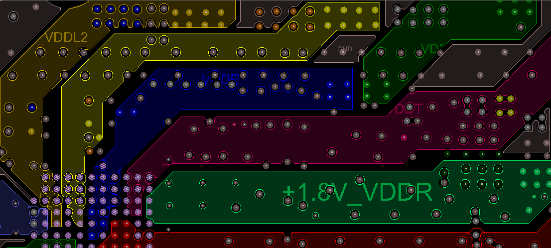
- Power supply planes
- Ensure sufficient lateral spacing between two power planes (about 3x the thickness of the plane is recommended)
- Insert ground plane between adjacent power planes where possible
 Figure 156. Example Power Plane Routing
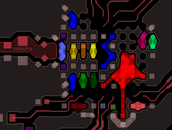
- Bypass Capacitors
- Use bypass capacitors with in-pad vias and place between the pin and the power plane. Avoid sharing ground vias or pads of bypass caps used for different power rails
- Minimize stubs on bypass capacitors to avoid parasitic inductance
 Figure 157. Bypass Capacitors Placed on the Power Supply Pin with In-pad Vias
- High speed SerDes traces
- Route all SerDes traces straight and minimized sharp curves or serpentines. Route for best signal integrity
- Some skew between SerDes traces can be tolerated. It is recommended to limit skew between traces to 320ps or less
- Place ground planes between the SerDes traces for improved isolation
 Figure 158. Layout Example of High Speed SerDes Traces
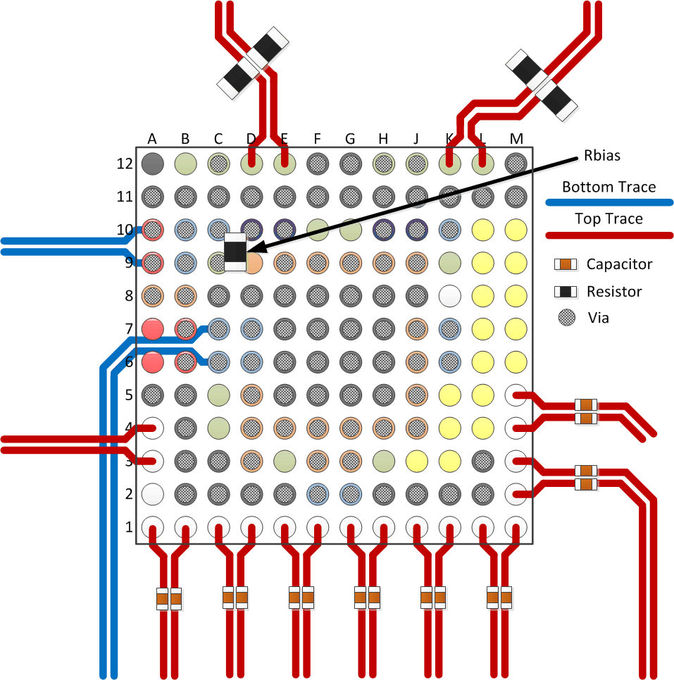
11.2 Layout Example
 Figure 159. Layout Example of DAC38RFxx