ZHCSOM0 October 2020 DAC43401-Q1 , DAC53401-Q1
PRODUCTION DATA
- 1 特性
- 2 应用
- 3 说明
- 4 Revision History
- 5 Device Comparison Table
- 6 Pin Configuration and Functions
-
7 Specifications
- 7.1 Absolute Maximum Ratings
- 7.2 ESD Ratings
- 7.3 Recommended Operating Conditions
- 7.4 Thermal Information
- 7.5 Electrical Characteristics
- 7.6 Timing Requirements: I2C Standard Mode
- 7.7 Timing Requirements: I2C Fast Mode
- 7.8 Timing Requirements: I2C Fast Mode Plus
- 7.9 Typical Characteristics: VDD = 1.8 V (Reference = VDD) or VDD = 2 V (Internal Reference)
- 7.10 Typical Characteristics: VDD = 5.5 V (Reference = VDD) or VDD = 5 V (Internal Reference)
- 7.11 Typical Characteristics
-
8 Detailed Description
- 8.1 Overview
- 8.2 Functional Block Diagram
- 8.3 Feature Description
- 8.4 Device Functional Modes
- 8.5 Programming
- 8.6
Register Map
- 8.6.1 STATUS Register (address = D0h) [reset = 000Ch or 0014h]
- 8.6.2 GENERAL_CONFIG Register (address = D1h) [reset = 01F0h]
- 8.6.3 TRIGGER Register (address = D3h) [reset = 0008h]
- 8.6.4 DAC_DATA Register (address = 21h) [reset = 0000h]
- 8.6.5 DAC_MARGIN_HIGH Register (address = 25h) [reset = 0000h]
- 8.6.6 DAC_MARGIN_LOW Register (address = 26h) [reset = 0000h]
- 8.6.7 PMBUS_OPERATION Register (address = 01h) [reset = 0000h]
- 8.6.8 PMBUS_STATUS_BYTE Register (address = 78h) [reset = 0000h]
- 8.6.9 PMBUS_VERSION Register (address = 98h) [reset = 2200h]
- 9 Application and Implementation
- 10Power Supply Recommendations
- 11Layout
- 12Device and Documentation Support
- 13Mechanical, Packaging, and Orderable Information
8.3.5 Power-on-Reset (POR)
The DACx3401-Q1 family of devices includes a power-on reset (POR) function that controls the output voltage at power up. After the VDD supply has been established, a POR event is issued. The POR causes all registers to initialize to default values, and communication with the device is valid only after a 30-ms, POR delay. The default value for all the registers in the DACx3401-Q1 is loaded from NVM as soon as the POR event is issued.
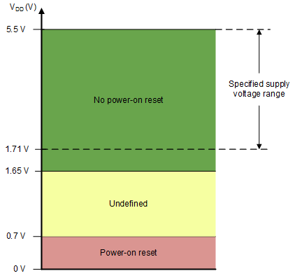
When the device powers up, a POR circuit sets the device to the default mode. The POR circuit requires specific VDD levels, as indicated in Figure 8-1, in order to make sure that the internal capacitors discharge and reset the device on power up. To make sure that a POR occurs, VDD must be less than 0.7 V for at least 1 ms. When VDD drops to less than 1.65 V, but remains greater than 0.7 V (shown as the undefined region), the device may or may not reset under all specified temperature and power-supply conditions. In this case, initiate a POR. When VDD remains greater than 1.65 V, a POR does not occur.
 Figure 8-1 Threshold Levels for VDD POR Circuit