ZHCSK27A July   2019  – December 2019 DAC43401 , DAC53401

PRODUCTION DATA.  

  1. 特性
  2. 应用
  3. 说明
    1.     Device Images
      1.      功能方框图
      2.      使用 DACx3401 的电源控制
  4. 修订历史记录
  5. Device Comparison Table
  6. Pin Configuration and Functions
    1.     Pin Functions
  7. Specifications
    1. 7.1  Absolute Maximum Ratings
    2. 7.2  ESD Ratings
    3. 7.3  Recommended Operating Conditions
    4. 7.4  Thermal Information
    5. 7.5  Electrical Characteristics
    6. 7.6  Timing Requirements: I2CTM Standard mode
    7. 7.7  Timing Requirements: I2CTM Fast mode
    8. 7.8  Timing Requirements: I2CTM Fast+ mode
    9. 7.9  Typical Characteristics: VDD = 1.8 V (Reference = VDD) or VDD = 2 V (Internal Reference)
    10. 7.10 Typical Characteristics: VDD = 5.5 V (Reference = VDD) or VDD = 5 V (Internal Reference)
    11. 7.11 Typical Characteristics
  8. Detailed Description
    1. 8.1 Overview
    2. 8.2 Functional Block Diagram
    3. 8.3 Feature Description
      1. 8.3.1 Digital-to-Analog Converter (DAC) Architecture
        1. 8.3.1.1 Reference Selection and DAC Transfer Function
          1. 8.3.1.1.1 Power Supply as Reference
          2. 8.3.1.1.2 Internal Reference
      2. 8.3.2 DAC Update
        1. 8.3.2.1 DAC Update Busy
      3. 8.3.3 Nonvolatile Memory (EEPROM or NVM)
        1. 8.3.3.1 NVM Cyclic Redundancy Check
        2. 8.3.3.2 NVM_CRC_ALARM_USER Bit
        3. 8.3.3.3 NVM_CRC_ALARM_INTERNAL Bit
      4. 8.3.4 Programmable Slew Rate
      5. 8.3.5 Power-on-Reset (POR)
      6. 8.3.6 Software Reset
      7. 8.3.7 Device Lock Feature
      8. 8.3.8 PMBus Compatibility
    4. 8.4 Device Functional Modes
      1. 8.4.1 Power Down Mode
      2. 8.4.2 Continuous Waveform Generation (CWG) Mode
      3. 8.4.3 PMBus Compatibility Mode
      4. 8.4.4 Medical Alarm Generation Mode
        1. 8.4.4.1 Low-Priority Alarm
        2. 8.4.4.2 Medium-Priority Alarm
        3. 8.4.4.3 High-Priority Alarm
        4. 8.4.4.4 Interburst Time
        5. 8.4.4.5 Pulse Off Time
        6. 8.4.4.6 Pulse On Time
    5. 8.5 Programming
      1. 8.5.1 F/S Mode Protocol
      2. 8.5.2 DACx3401 I2C Update Sequence
      3. 8.5.3 Address Byte
      4. 8.5.4 Command Byte
      5. 8.5.5 I2C Read Sequence
    6. 8.6 Register Map
      1. 8.6.1  STATUS Register (address = D0h) (reset = 000Ch or 0014h)
        1. Table 18. STATUS Register Field Descriptions
      2. 8.6.2  GENERAL_CONFIG Register (address = D1h) (reset = 01F0h)
        1. Table 19. GENERAL_CONFIG Register Field Descriptions
      3. 8.6.3  MED_ALARM_CONFIG Register (address = D2h) (reset = 0000h)
        1. Table 20. MED_ALARM_CONFIG Register Field Descriptions
      4. 8.6.4  TRIGGER Register (address = D3h) (reset = 0008h)
        1. Table 21. TRIGGER Register Field Descriptions
      5. 8.6.5  DAC_DATA Register (address = 21h) (reset = 0000h)
        1. Table 22. DAC_DATA Register Field Descriptions
      6. 8.6.6  DAC_MARGIN_HIGH Register (address = 25h) (reset = 0000h)
        1. Table 23. DAC_MARGIN_HIGH Register Field Descriptions
      7. 8.6.7  DAC_MARGIN_LOW Register (address = 26h) (reset = 0000h)
        1. Table 24. DAC_MARGIN_LOW Register Field Descriptions
      8. 8.6.8  PMBUS_OPERATION Register (address = 01h) (reset = 0000h)
        1. Table 25. PMBUS_OPERATION Register Field Descriptions
      9. 8.6.9  PMBUS_STATUS_BYTE Register (address = 78h) (reset = 0000h)
        1. Table 26. PMBUS_STATUS_BYTE Register Field Descriptions
      10. 8.6.10 PMBUS_VERSION Register (address = 98h) (reset = 2200h)
        1. Table 27. PMBUS_VERSION Register Field Descriptions
  9. Application and Implementation
    1. 9.1 Application Information
    2. 9.2 Typical Applications
      1. 9.2.1 Programmable LED Biasing
        1. 9.2.1.1 Design Requirements
        2. 9.2.1.2 Detailed Design Procedure
        3. 9.2.1.3 Application Curves
      2. 9.2.2 Power-Supply Margining
        1. 9.2.2.1 Design Requirements
        2. 9.2.2.2 Detailed Design Procedure
        3. 9.2.2.3 Application Curves
      3. 9.2.3 Medical Alarm Generation
        1. 9.2.3.1 Design Requirements
        2. 9.2.3.2 Detailed Design Procedure
        3. 9.2.3.3 Application Curves
  10. 10Power Supply Recommendations
  11. 11Layout
    1. 11.1 Layout Guidelines
    2. 11.2 Layout Example
  12. 12器件和文档支持
    1. 12.1 文档支持
      1. 12.1.1 相关文档
    2. 12.2 相关链接
    3. 12.3 接收文档更新通知
    4. 12.4 支持资源
    5. 12.5 商标
    6. 12.6 静电放电警告
    7. 12.7 Glossary
  13. 13机械、封装和可订购信息

封装选项

机械数据 (封装 | 引脚)
散热焊盘机械数据 (封装 | 引脚)
订购信息

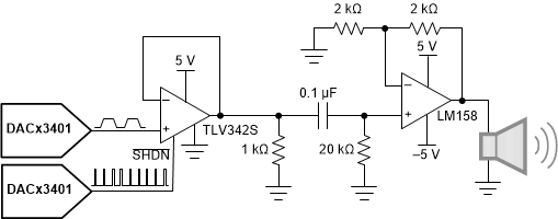
Medical Alarm Generation

All medical devices implementing an alarm system shall comply to IEC60601-1-8 standard for medical alarms (as per IEC60601-1 Ed 3.1). The regulatory tests are done at a system level; therefore, system level acoustics play a major role in the compliance. A medical alarm is a common functional block in many medical devices. A portable implementation is needed that can also be customized to fit mechanical and audio or acoustic requirements. The DACx3401-based design is aimed at providing a programmable, standalone, and robust implementation at a very low cost.

There are three types of alarms with different timing requirements: low priority, medium priority, and high priority. Usually, for easy identification, different timings are employed for different equipment. Medical device manufacturers prefer using their signature melodies within the limits of the standard.
DAC53401 DAC43401 dacx3401-medical-alarm.gifFigure 70. Medical Alarm