ZHCSM38 december 2020 DAC43701 , DAC53701
PRODUCTION DATA
- 1
- 1 特性
- 2 应用
- 3 说明
- 4 Revision History
- 5 Device Comparison Table
- 6 Pin Configuration and Functions
-
7 Specifications
- 7.1 Absolute Maximum Ratings
- 7.2 ESD Ratings
- 7.3 Recommended Operating Conditions
- 7.4 Thermal Information
- 7.5 Electrical Characteristics
- 7.6 Timing Requirements: I2C Standard Mode
- 7.7 Timing Requirements: I2C Fast Mode
- 7.8 Timing Requirements: I2C Fast Mode Plus
- 7.9 Timing Requirements: GPI
- 7.10 Timing Diagram
- 7.11 Typical Characteristics: VDD = 5.5 V (Reference = VDD) or VDD = 5 V (Internal Reference)
- 7.12 Typical Characteristics: VDD = 1.8 V (Reference = VDD) or VDD = 2 V (Internal Reference)
- 7.13 Typical Characteristics
-
8 Detailed Description
- 8.1 Overview
- 8.2 Functional Block Diagram
- 8.3 Feature Description
- 8.4 Device Functional Modes
- 8.5 Programming
- 8.6
Register Map
- 8.6.1 STATUS Register (address = D0h) [reset = 000Ch or 0014h]
- 8.6.2 GENERAL_CONFIG Register (address = D1h) [reset = 01F0h]
- 8.6.3 CONFIG2 Register (address = D2h) [reset = 0000h]
- 8.6.4 TRIGGER Register (address = D3h) [reset = 0008h]
- 8.6.5 DAC_DATA Register (address = 21h) [reset = 0000h]
- 8.6.6 DAC_MARGIN_HIGH Register (address = 25h) [reset = 0000h]
- 8.6.7 DAC_MARGIN_LOW Register (address = 26h) [reset = 0000h]
- 8.6.8 PMBUS_OPERATION Register (address = 01h) [reset = 0000h]
- 8.6.9 PMBUS_STATUS_BYTE Register (address = 78h) [reset = 0000h]
- 8.6.10 PMBUS_VERSION Register (address = 98h) [reset = 2200h]
- 9 Application and Implementation
- 10Power Supply Recommendations
- 11Layout
- 12Device and Documentation Support
- 13Mechanical, Packaging, and Orderable Information
8.5.2 I2C Update Sequence
| MSB | .... | LSB | ACK | MSB | ... | LSB | ACK | MSB | ... | LSB | ACK | MSB | ... | LSB | ACK |
|---|---|---|---|---|---|---|---|---|---|---|---|---|---|---|---|
| Address (A) byte Section 8.5.2.1 |
Command byte Section 8.5.2.2 |
Data byte - MSDB | Data byte - LSDB | ||||||||||||
| DB [31:24] | DB [23:16] | DB [15:8] | DB [7:0] | ||||||||||||
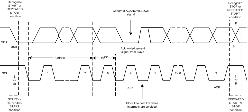
After each byte is received, the DACx3701 family acknowledges the byte by pulling the SDA line low during the high period of a single clock pulse, as shown in Figure 8-6. These four bytes and acknowledge cycles make up the 36 clock cycles required for a single update to occur. A valid I2C address byte selects the DACx3701 devices.
 Figure 8-6 I2C Bus
Protocol
Figure 8-6 I2C Bus
ProtocolThe command byte sets the operating mode of the selected DACx3701 device. For a data update to occur when the operating mode is selected by this byte, the DACx3701 device must receive two data bytes: the most significant data byte (MSDB) and least significant data byte (LSDB). The DACx3701 device performs an update on the falling edge of the acknowledge signal that follows the LSDB.
When using fast mode (clock = 400 kHz), the maximum DAC update rate is limited to 10 kSPS. Using the fast mode plus (clock = 1 MHz), the maximum DAC update rate is limited to 25 kSPS. When a stop condition is received, the DACx3701 device releases the I2C bus and awaits a new start condition.