SGLS387H July 2007 – August 2016 DAC5675A-SP
PRODUCTION DATA.
- 1 Features
- 2 Applications
- 3 Description
- 4 Revision History
- 5 Description (continued)
- 6 Pin Configuration and Functions
-
7 Specifications
- 7.1 Absolute Maximum Ratings
- 7.2 ESD Ratings
- 7.3 Recommended Operating Conditions
- 7.4 Thermal Information
- 7.5 DC Electrical Characteristics (Unchanged After 100 kRad)
- 7.6 AC Electrical Characteristics (Unchanged After 100 kRad)
- 7.7 Digital Specifications (Unchanged After 100 kRad)
- 7.8 Electrical Characteristics
- 7.9 Typical Characteristics
- 8 Detailed Description
- 9 Application and Implementation
- 10Power Supply Recommendations
- 11Layout
- 12Device and Documentation Support
- 13Mechanical, Packaging, and Orderable Information
8 Detailed Description
8.1 Overview
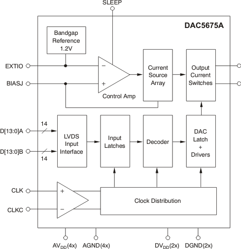
Functional Block Diagram shows a simplified block diagram of the current steering DAC5675A-SP. The DAC5675A-SP consists of a segmented array of NPN-transistor current sources, capable of delivering a full-scale output current up to 20 mA. Differential current switches direct the current of each current source to either one of the complementary output nodes IOUT1 or IOUT2. The complementary current output enables differential operation, canceling out common-mode noise sources (digital feedthrough, on-chip, and PCB noise), dc offsets, and even-order distortion components, and doubling signal output power.
The full-scale output current is set using an external resistor (RBIAS) with an on-chip bandgap voltage reference source (1.2 V) and control amplifier. The current (IBIAS) through resistor RBIAS is mirrored internally to provide a full-scale output current equal to 16 × IBIAS. The full-scale current is adjustable from 20 to 2 mA by using the appropriate bias resistor value.
8.2 Functional Block Diagram
8.3 Feature Description
8.3.1 Digital Inputs
The DAC5675A-SP uses a low-voltage differential signaling (LVDS) bus input interface. The LVDS features a low differential voltage swing with low constant power consumption (4 mA per complementary data input) across frequency. The differential characteristic of LVDS allows for high-speed data transmission with low electromagnetic interference (EMI) levels. Figure 12 shows the equivalent complementary digital input interface for the DAC5675A-SP, valid for pins D[13:0]A and D[13:0]B. Note that the LVDS interface features internal 110-Ω resistors for proper termination. Figure 2 shows the LVDS input timing measurement circuit and waveforms. A common-mode level of 1.2 V and a differential input swing of 0.8 VPP is applied to the inputs.
Figure 13 shows a schematic of the equivalent CMOS/TTL-compatible digital inputs of the DAC5675A-SP, valid for the SLEEP pin.
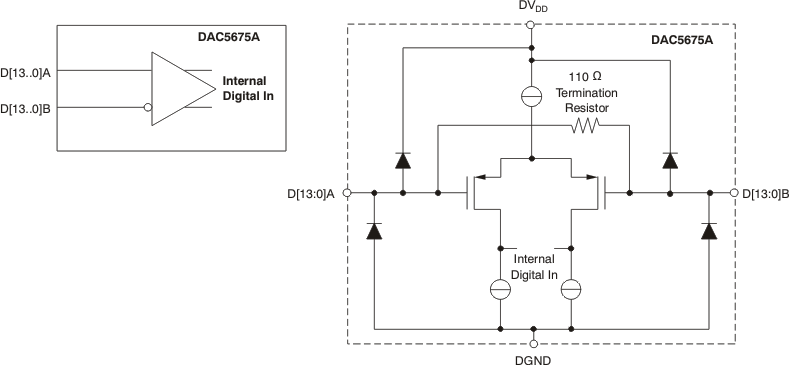 Figure 12. LVDS Digital Equivalent Input
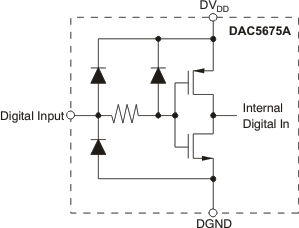 Figure 13. CMOS/TTL Digital Equivalent Input
8.3.2 Clock Input
The DAC5675A-SP features differential LVPECL-compatible clock inputs (CLK, CLKC). Figure 14 shows the equivalent schematic of the clock input buffer. The internal biasing resistors set the input common-mode voltage to approximately 2 V, while the input resistance is typically 670 Ω. A variety of clock sources can be ac-coupled to the device, including a sine-wave source (see Figure 15).
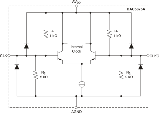 Figure 14. Clock Equivalent Input
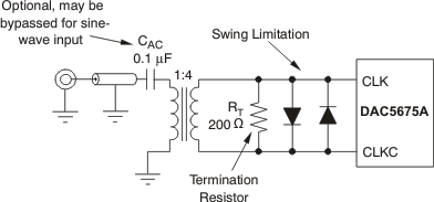 Figure 15. Driving the DAC5675A-SP With a Single-Ended Clock Source Using a Transformer
To obtain best ac performance, the DAC5675A-SP clock input should be driven with a differential LVPECL or sine-wave source as shown in Figure 16 and Figure 17. Here, the potential of VTT should be set to the termination voltage required by the driver along with the proper termination resistors (RT). The DAC5675A-SP clock input can also be driven single ended (see Figure 18).
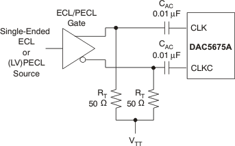 Figure 16. Driving the DAC5675A-SP With a Single-Ended ECL/PECL Clock Source
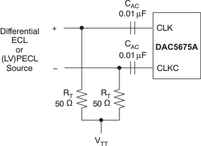 Figure 17. Driving the DAC5675A-SP With a Differential ECL/PECL Clock Source
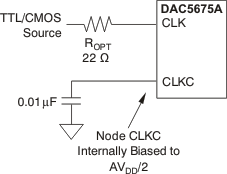 Figure 18. Driving the DAC5675A-SP With a Single-Ended TTL/CMOS Clock Source
8.3.3 Supply Inputs
The DAC5675A-SP comprises separate analog and digital supplies, AVDD and DVDD, respectively. These supply inputs can be set independently from 3.6 to 3.15 V.
8.3.4 DAC Transfer Function
The DAC5675A-SP has a current sink output. The current flow through IOUT1 and IOUT2 is controlled by D[13:0]A and D[13:0]B. For ease of use, D[13:0] is denoted as the logical bit equivalent of D[13:0]A and its complement D[13:0]B. The DAC5675A-SP supports straight binary coding with D13 being the MSB and D0 the LSB. Full-scale current flows through IOUT2 when all D[13:0] inputs are set high and through IOUT1 when all D[13:0] inputs are set low. The relationship between IOUT1 and IOUT2 can be expressed as Equation 1.

IO(FS) is the full-scale output current sink (2 to 20 mA). Because the output stage is a current sink, the current can only flow from AVDD through the load resistors RL into the IOUT1 and IOUT2 pins.
The output current flow in each pin driving a resistive load can be expressed as shown in Figure 19, Equation 2, and Equation 3.
![DAC5675A-SP Relationship Between
D[13:0], IOUT1 and IOUT2 DAC5675A-SP dac-xfer_gls387.gif](/ods/images/SGLS387H/dac-xfer_gls387.gif) Figure 19. Relationship Between D[13:0], IOUT1 and IOUT2
Figure 19. Relationship Between D[13:0], IOUT1 and IOUT2


where
- CODE is the decimal representation of the DAC input word
This would translate into single-ended voltages at IOUT1 and IOUT2, as shown in Equation 4 and Equation 5.
Assuming that D[13:0] = 1 and the RL is 50 Ω, the differential voltage between pins IOUT1 and IOUT2 can be expressed as shown in Equation 6 through Equation 8.
If D[13:0] = 0, then IOUT2 = 0 mA, IOUT1 = 20 mA, and the differential voltage VDIFF = –1 V.
The output currents and voltages in IOUT1 and IOUT2 are complementary. The voltage, when measured differentially, is doubled compared to measuring each output individually. Take care not to exceed the compliance voltages at the IOUT1 and IOUT2 pins to keep signal distortion low.
8.3.5 Reference Operation
The DAC5675A-SP has a bandgap reference and control amplifier for biasing the full-scale output current. The full-scale output current is set by applying an external resistor, RBIAS. The bias current IBIAS through resistor RBIAS is defined by the on-chip bandgap reference voltage and control amplifier. The full-scale output current equals 16× this bias current. The full-scale output current IO(FS) is thus expressed as Equation 9.

where
- VEXTIO is the voltage at pin EXTIO
The bandgap reference voltage delivers a stable voltage of 1.2 V. This reference can be overridden by applying an external voltage to terminal EXTIO. The bandgap reference can additionally be used for external reference operation. In such a case, select an external buffer amplifier with high-impedance input to limit the bandgap load current to less than 100 nA. The capacitor CEXT may be omitted. Pin EXTIO serves as either an input or output node. The full-scale output current is adjustable from 20 to 2 mA by varying resistor RBIAS.
8.3.6 Analog Current Outputs
Figure 20 shows a simplified schematic of the current source array output with corresponding switches. Differential NPN switches direct the current of each individual NPN current source to either the positive output node IOUT1 or its complementary negative output node IOUT2. The output impedance is determined by the stack of the current sources and differential switches and is >300 kΩ in parallel with 5-pF output capacitance.
The external output resistors are referred to the positive supply, AVDD.
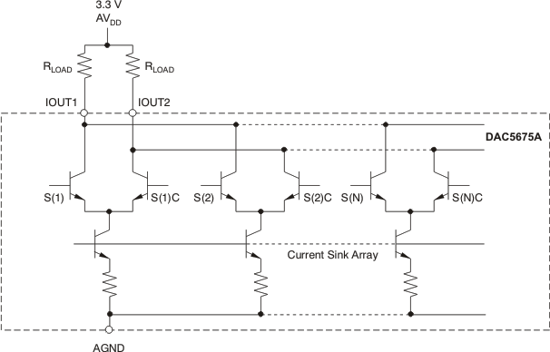 Figure 20. Equivalent Analog Current Output
Figure 21(a) shows the typical differential output configuration with two external matched resistor loads. The nominal resistor load of 25 Ω gives a differential output swing of 1 VPP (0.5 VPP single ended) when applying a 20-mA full-scale output current. The output impedance of the DAC5675A-SP slightly depends on the output voltage at nodes IOUT1 and IOUT2. Consequently, for optimum dc-integral nonlinearity, choose the configuration of Figure 21(b). In this current/voltage (I-V) configuration, terminal IOUT1 is kept at AVDD by the inverting operational amplifier. The complementary output should be connected to AVDD to provide a dc-current path for the current sources switched to IOUT1. The amplifier maximum output swing and the full-scale output current of the DAC determine the value of the feedback resistor, RFB. The capacitor CFB filters the steep edges of the DAC5675A-SP current output, thereby reducing the operational amplifier slew-rate requirements. In this configuration, the operational amplifier should operate at a supply voltage higher than the resistor output reference voltage AVDD as a result of its positive and negative output swing around AVDD. Select node IOUT1 if a single-ended unipolar output is desired.
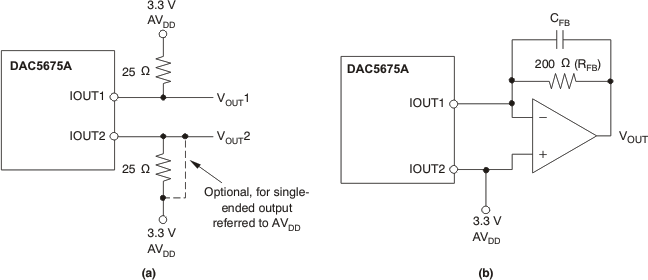 Figure 21. Output Configurations
8.4 Device Functional Modes
8.4.1 Sleep Mode
The DAC5675A-SP features a power-down mode that turns off the output current and reduces the supply current to approximately 6 mA. The power-down mode is activated by applying a logic level one to the SLEEP pin, pulled down internally.