ZHCSEG7A December 2015 – January 2016 DAC60096
PRODUCTION DATA.
- 1 特性
- 2 应用
- 3 说明
- 4 修订历史记录
- 5 Pin Configuration and Functions
-
6 Specifications
- 6.1 Absolute Maximum Ratings
- 6.2 ESD Ratings
- 6.3 Recommended Operating Conditions
- 6.4 Thermal Information
- 6.5 Electrical Characteristics: DAC DC
- 6.6 Electrical Characteristics: Square-Wave Output
- 6.7 Electrical Characteristics: General
- 6.8 Timing Requirements
- 6.9 Typical Characteristics: DC Mode
- 6.10 Typical Characteristics: Toggle Mode
- 6.11 Typical Characteristics, General
-
7 Detailed Description
- 7.1 Overview
- 7.2 Functional Block Diagram
- 7.3 Feature Description
- 7.4 Device Functional Modes
- 7.5 Programming
- 7.6
Register Maps
- 7.6.1 8.5.1 BUFA Register (address = 0x0) [reset = 0x0000]
- 7.6.2 BUFB Register (address = 0x1) [reset = 0x0000]
- 7.6.3 CON Register (address = 0x4) [reset = 0x0555]
- 7.6.4 CRC Register (address = 0x5) [reset = 0xFFF]
- 7.6.5 PTR Register (address = 0x6) [reset = 0x0000]
- 7.6.6 SWR Register (address = 0x7) [reset = 0x0000]
- 7.6.7 PWRM Register (address = 0x6) [reset = 0xCAFE]
- 7.6.8 SDIV Register (address = 0x9) [reset = 0x0000]
- 8 Application and Implementation
- 9 Power Supply Recommendations
- 10Layout
- 11器件和文档支持
- 12机械、封装和可订购信息
10 Layout
10.1 Layout Guidelines
- Bypass all power-supply pins to ground with a low ESR ceramic bypass capacitor. The typical recommended bypass capacitance is 0.1-µF to 0.22-µF ceramic with a X7R or NP0 dielectric.
- Place power supplies and VREFH/L bypass capacitors close to pins to minimize inductance and optimize performance. Inner supply and reference pads can connect to the bypass arrangement on the bottom layer of the PCB through vias to minimize trace length. This is illustrated in Figure 56 and Figure 59.
- Include a 100-nF bypass capacitor for both internal reference inputs between this pin and their respective ground pins.
- Use a high-quality ceramic type NP0 or X7R for optimal performance across temperature, and low dissipation factor.
- Make sure that the digital and analog sections have proper placement with respect to the digital pins and analog pins of the DAC60096 device. The separation of analog and digital blocks allow for better design and practice because it reduces coupling into neighboring blocks, and minimizes the interaction between analog and digital return currents.
10.2 Layout Examples
10.2.1 Optimal Layout Example
Optimal layout requires the addition of blind vias. This layout reduces trace length and brings the bypass capacitor arrangements closer to the device pads. Figure 56 to Figure 59 show the board layouts.
Figure 56. DAC60096 Example Board Layout – Top Layer PCB
Figure 57. DAC60096 Example Board Layout – Internal AVCC and AVSS Plane
Figure 58. DAC60096 Example Board Layout – DVDD Internal Plane With Select DAC Outputs
Figure 59. DAC60096 Example Board Layout – Bottom Layer PCB.
(A): Bypass Capacitor Arrangement; (B) Polygon Pours; (C) PAD With Pours
(A): Bypass Capacitor Arrangement; (B) Polygon Pours; (C) PAD With Pours
10.2.2 Standard Layout Example
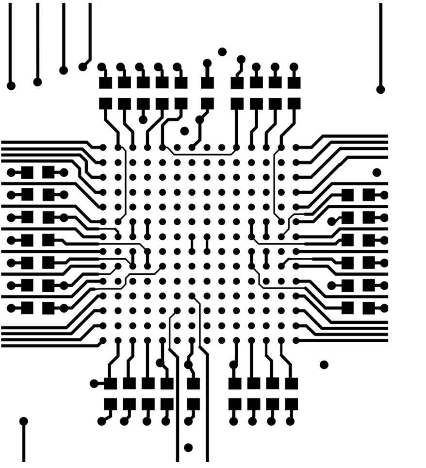
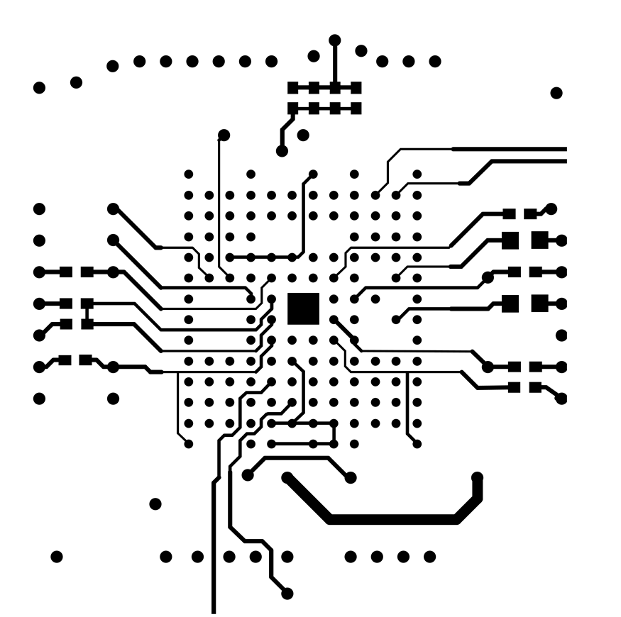
Only through-hole vias are included in this layout. Bypass capacitors are placed as close to their respective device pads. Bottom bypass brought out from device. This layout can lead to increased trace length, which will increase the series inductance of the net making it more susceptible to noise and voltage spikes. Figure 60 to Figure 61 show the board layouts.
 Figure 60. DAC60096 Example Board Layout – Top Layer
 Figure 61. DAC60096 Example Board Layout – Bottom Layer