ZHCSEG7A December 2015 – January 2016 DAC60096
PRODUCTION DATA.
- 1 特性
- 2 应用
- 3 说明
- 4 修订历史记录
- 5 Pin Configuration and Functions
-
6 Specifications
- 6.1 Absolute Maximum Ratings
- 6.2 ESD Ratings
- 6.3 Recommended Operating Conditions
- 6.4 Thermal Information
- 6.5 Electrical Characteristics: DAC DC
- 6.6 Electrical Characteristics: Square-Wave Output
- 6.7 Electrical Characteristics: General
- 6.8 Timing Requirements
- 6.9 Typical Characteristics: DC Mode
- 6.10 Typical Characteristics: Toggle Mode
- 6.11 Typical Characteristics, General
-
7 Detailed Description
- 7.1 Overview
- 7.2 Functional Block Diagram
- 7.3 Feature Description
- 7.4 Device Functional Modes
- 7.5 Programming
- 7.6
Register Maps
- 7.6.1 8.5.1 BUFA Register (address = 0x0) [reset = 0x0000]
- 7.6.2 BUFB Register (address = 0x1) [reset = 0x0000]
- 7.6.3 CON Register (address = 0x4) [reset = 0x0555]
- 7.6.4 CRC Register (address = 0x5) [reset = 0xFFF]
- 7.6.5 PTR Register (address = 0x6) [reset = 0x0000]
- 7.6.6 SWR Register (address = 0x7) [reset = 0x0000]
- 7.6.7 PWRM Register (address = 0x6) [reset = 0xCAFE]
- 7.6.8 SDIV Register (address = 0x9) [reset = 0x0000]
- 8 Application and Implementation
- 9 Power Supply Recommendations
- 10Layout
- 11器件和文档支持
- 12机械、封装和可订购信息
6 Specifications
6.1 Absolute Maximum Ratings
over operating free-air temperature range (unless otherwise noted)(1)| MIN | MAX | UNIT | ||
|---|---|---|---|---|
| Supply voltage | AVCC to DGND | –0.3 | 13 | V |
| AVSS to DGND | –13 | 0.3 | ||
| DVDD to DGND | –0.3 | 6 | ||
| AVCC to AVSS | –0.3 | 26 | ||
| DGND to AGND | –0.3 | 0.3 | ||
| DGND to REFGND[1,2] | –0.3 | 0.3 | ||
| Pin voltage | REF1 to REFGND1 | –0.3 | 6 | V |
| REF2 to REFGND2 | –0.3 | 6 | ||
| DAC to DGND | AVSS – 0.3 | AVCC + 0.3 | ||
| CLEAR, CS, LDAC, RESET, SCLK, SDI, SDO, TRIGG, STATS to DGND | –0.3 | DVDD + 0.3 | ||
| VREFH to DGND | –0.3 | AVCC + 0.3 | ||
| VREFL to DGND | AVSS – 0.3 | 0.3 | ||
| VREFH to adjacent VREFL | –0.3 | 26 | ||
| Temperature | Operating, TA | –40 | 85 | °C |
| Junction, TJ | –40 | 150 | ||
| Storage, Tstg | –40 | 150 | ||
(1) Stresses beyond those listed under Absolute Maximum Ratings may cause permanent damage to the device. These are stress ratings only, which do not imply functional operation of the device at these or any other conditions beyond those indicated under Recommended Operating Conditions. Exposure to absolute-maximum-rated conditions for extended periods may affect device reliability.
6.2 ESD Ratings
| VALUE | UNIT | |||
|---|---|---|---|---|
| V(ESD) | Electrostatic discharge | Human-body model (HBM), per ANSI/ESDA/JEDEC JS-001(1) | ±2000 | V |
| Charged-device model (CDM), per JEDEC specification JESD22-C101(2) | ±500 | |||
(1) JEDEC document JEP155 states that 500-V HBM allows safe manufacturing with a standard ESD control process.
(2) JEDEC document JEP157 states that 250-V CDM allows safe manufacturing with a standard ESD control process.
6.3 Recommended Operating Conditions
over operating free-air temperature range (unless otherwise noted)| MIN | NOM | MAX | UNIT | ||||
|---|---|---|---|---|---|---|---|
| POWER SUPPLY | |||||||
| AVCC | 11.2 | 12 | 12.6 | V | |||
| AVSS | –12.6 | –12 | –11.2 | V | |||
| DVDD | 3 | 3.3 | 5.5 | V | |||
| AVCC to AVSS | 22.4 | 24 | 25.2 | V | |||
| DIGITAL INPUTS | |||||||
| Digital input voltage | 0 | DVDD | V | ||||
| REFERENCE INPUT | |||||||
| Reference input voltage, VREF | 2.475 | 2.5 | 2.525 | V | |||
| TEMPERATURE | |||||||
| Operating ambient temperature, TA | –40 | 85 | °C | ||||
6.4 Thermal Information
| THERMAL METRIC(1) | DAC60096 | UNIT | |
|---|---|---|---|
| ZEB (NFBGA) | |||
| 196 BALLS | |||
| RθJA | Junction-to-ambient thermal resistance | 21.4 | °C/W |
| RθJC(top) | Junction-to-case (top) thermal resistance | 7.5 | °C/W |
| RθJB | Junction-to-board thermal resistance | 5.1 | °C/W |
| ψJT | Junction-to-top characterization parameter | 0.4 | °C/W |
| ψJB | Junction-to-board characterization parameter | 5.0 | °C/W |
| RθJC(bot) | Junction-to-case (bottom) thermal resistance | N/A | °C/W |
(1) For more information about traditional and new thermal metrics, see the Semiconductor and IC Package Thermal Metrics application report, SPRA953.
6.5 Electrical Characteristics: DAC DC
at AVCC = 11.2 V to 12.6 V, AVSS = –12.6 V to –11.2 V, DVDD = 3 V to 5.5 V, AGND = DGND = REFGND[1,2] = 0 V, REF1 = REF2 = 2.5 V (specifications exclude any reference contributions), no load on DACs, and TA = –40°C to +85°C (unless otherwise noted)| PARAMETER | TEST CONDITIONS | MIN | TYP | MAX | UNIT | |
|---|---|---|---|---|---|---|
| STATIC PERFORMANCE | ||||||
| Resolution | 12 | Bits | ||||
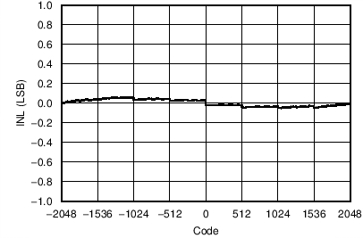
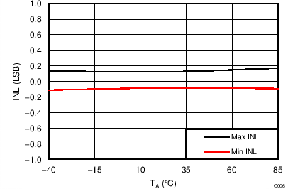
| INL | Relative accuracy | ±0.15 | ±1 | LSB | ||
| DNL | Differential nonlinearity | Specified 12-bit monotonic | ±0.1 | ±0.9 | LSB | |
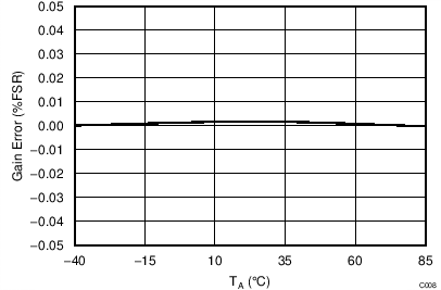
| Gain error | TA = 25°C | ±0.05 | ±0.15 | %FSR | ||
| Zero-code error | TA = 25°C, code 000h | ±2 | ±7 | mV | ||
| Gain error drift | ±1 | ppm/°C | ||||
| Zero-code error drift | ±1 | ppm/°C | ||||
| OUTPUT CHARACTERISTICS | ||||||
| Output voltage | –10.5 | 10.5 | V | |||
| Output impedance | 41 | kΩ | ||||
| DC crosstalk | Measured channel at code 000h, all others transition from code 7FFh to 02Bh | 0.5 | LSB | |||
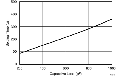
| Settling time | DAC ouput transition: code 800h to 7FFh to within 1 LSB, 6x load: R(SERIES) = 17 kΩ, CLOAD = 300 pF |
160 | µs | |||
| DAC ouput transition: code 800h to 7FFh to within 1 LSB, 1x load: R(SERIES) = 100 kΩ, CLOAD = 50 pF |
65 | |||||
| Output noise | TA = 25°C, 1 kHz, code 000h | 60 | nV/√Hz | |||
6.6 Electrical Characteristics: Square-Wave Output
at AVCC = 11.2 V to 12.6 V, AVSS = –12.6 V to –11.2 V, DVDD = 3 V to 5.5 V, AGND = DGND = REFGND[1,2] = 0 V, REF1 = REF2 = 2.5 V (specifications exclude any reference contributions), no load on DACs, and TA = –40°C to +85°C (unless otherwise noted)| PARAMETER | TEST CONDITIONS | MIN | TYP | MAX | UNIT | |
|---|---|---|---|---|---|---|
| DAC OUTPUTS – 6x LOAD: R(SERIES) = 17 kΩ, CLOAD = 300 pF | ||||||
| Frequency | For amplitude ≥ 9.1 VRMS, amplitude = ±10.5 VPP, codes 7FFh to 801h |
3 | kHz | |||
| Amplitude | Frequency = 3 kHz, amplitude = ±10.5 VPP, codes 7FFh to 801h |
9.1 | VRMS | |||
| Frequency = 5 kHz, amplitude = ±10.5 VPP, codes 7FFh to 801h |
8 | VRMS | ||||
| Amplitude step precision | Frequency = 3 kHz, amplitude ≥ 1 VRMS | 6 | mVRMS | |||
| Amplitude temperature drift | Frequency = 3 kHz, amplitude = ±5 VPP, codes 3CFh to C31h |
5 | mVRMS | |||
| Frequency = 3 kHz, amplitude = ±10.5 VPP, codes 7FFh to 801h |
15 | mVRMS | ||||
| Offset voltage | Frequency = 3 kHz, amplitude = ±5 VPP, codes 3CFh to C31h |
–10 | 10 | mV | ||
| Frequency = 3 kHz, amplitude = ±10.5 VPP, codes 7FFh to 801h |
–10 | 10 | mV | |||
| Rise and fall time | Frequency = 3 kHz, amplitude = ±10.5 VPP, 10% to 90%, codes 7FFh to 801h |
40 | µs | |||
| DAC OUTPUTS – 1x LOAD: R(SERIES) = 100 kΩ, CLOAD = 50 pF (1) | ||||||
| Frequency | For amplitude ≥ 9.1 VRMS, amplitude = ±10.5 VPP, codes 7FFh and 801h |
5 | kHz | |||
| Amplitude | Frequency = 3 kHz, amplitude = ±10.5 VPP, codes 7FFh to 801h |
10 | VRMS | |||
| Frequency = 5 kHz, amplitude = ±10.5 VPP, codes 7FFh to 801h |
9.5 | VRMS | ||||
| Amplitude step precision | Frequency = 3 kHz, amplitude ≥ 1 VRMS | 7 | mVRMS | |||
| Amplitude temperature drift | Frequency = 3 kHz, amplitude = ±5 VPP, codes 3CFh to C31h |
5 | mVRMS | |||
| Frequency = 3 kHz, amplitude = ±10.5 VPP, codes 7FFh to 801h |
15 | mVRMS | ||||
| Offset voltage | Frequency = 3 kHz, amplitude = ±5 VPP, codes 3CFh to C31h |
–10 | 10 | mV | ||
| Frequency = 3 kHz, amplitude = ±10.5 VPP, codes 7FFh to 801h |
–10 | 10 | mV | |||
| Rise and fall time | Frequency = 3 kHz, amplitude = ±10.5 VPP, 10% to 90%, codes 7FFh to 801h |
10 | µs | |||
(1) Specified by design and characterization. Not tested during production.
6.7 Electrical Characteristics: General
at AVCC = 11.2 V to 12.6 V, AVSS = –12.6 V to –11.2 V, DVDD = 3 V to 5.5 V, AGND = DGND = REFGND[1,2] = 0 V, REF1 = REF2 = 2.5 V (specifications exclude any reference contributions), no load on DACs, and TA = –40°C to +85°C (unless otherwise noted)| PARAMETER | TEST CONDITIONS | MIN | TYP | MAX | UNIT | |
|---|---|---|---|---|---|---|
| EXTERNAL REFERENCE INPUTS | ||||||
| VREF | Input voltage range | REF1 and REF2 input pins | 2.475 | 2.5 | 2.525 | V |
| Reference input current | Per input pin | 1 | µA | |||
| DIGITAL LOGIC | ||||||
| VIH | High-level input voltage | 0.7 × DVDD | V | |||
| VIL | Low-level input voltage | 0.3 × DVDD | V | |||
| VOH | High-level output voltage | ILOAD = 1 mA, SDO2x = 01 | DVDD - 0.2 | V | ||
| VOL | Low-level output voltage | ILOAD = –1 mA, SDO2x = 01 | 0.4 | V | ||
| Input capacitance | 20 | pF | ||||
| POWER REQUIREMENTS (1) | ||||||
| I(AVCC) | AVCC supply current | 6x load: R(SERIES) = 17 kΩ, CLOAD = 300 pF frequency = 3 kHz 48 DAC outputs, codes 7FFh and 801h 48 DAC outputs, codes 117h and EE9h |
18.1 | 25 | mA | |
| I(AVSS) | AVSS supply current | –25 | –18.1 | mA | ||
| I(DVDD) | DVDD supply current | 2 | 10 | mA | ||
| Power consumption | 440 | mW | ||||
| I(AVCC) | AVCC supply current | 1x load: R(SERIES) = 100 kΩ, CLOAD = 50 pF frequency = 3 kHz 48 DAC outputs, codes 7FFh and 801h 48 DAC outputs, codes 117h and EE9h (2) |
17 | 22 | mA | |
| I(AVSS) | AVSS supply current | –22 | –17 | mA | ||
| I(DVDD) | DVDD supply current | 2 | 10 | mA | ||
| Power consumption | 415 | mW | ||||
| I(AVCC) | AVCC supply current | 6x load: R(SERIES) = 17 kΩ, CLOAD = 300 pF frequency = 3 kHz All DAC outputs, codes 02Bh and FD5h |
25 | 30 | mA | |
| I(AVSS) | AVSS supply current | –30 | –25 | mA | ||
| I(DVDD) | DVDD supply current | 2 | 10 | mA | ||
| Power consumption | 650 | 760 | mW | |||
(1) Power requirements tested unloaded during production. Load current contribution to power consumption specified by design and characterization.
(2) Specified by design and characterization. Not tested during production.
6.8 Timing Requirements(1)(2)
at AVCC = 11.2 V to 12.6 V, AVSS = –12.6 V to –11.2 V, DVDD = 3 V to 5.5 V, AGND = DGND = REFGND[1,2] = 0 V, REF1 = REF2 = 2.5 V (specifications exclude any reference contributions), no load on DACs, and TA = –40°C to +85°C (unless otherwise noted)| MIN | NOM | MAX | UNIT | |||
|---|---|---|---|---|---|---|
| SERIAL INTERFACE – DEFAULT MODE: SDO2X = 01, PHAINV = 01 | ||||||
| fSCLK | SCLK frequency | Write operation | 32 | MHz | ||
| Read operation | 18 | MHz | ||||
| tPH | SCLK pulse width high | Write operation | 14 | ns | ||
| Read operation | 26 | ns | ||||
| tPL | SCLK pulse width low | Write operation | 14 | ns | ||
| Read operation | 26 | ns | ||||
| tSU | SDI setup | 5 | ns | |||
| tH | SDI hold | 10 | ns | |||
| tCSS | CS setup | 10 | ns | |||
| tCSH | CS hold | 20 | ns | |||
| tIAG | Inter-access gap | 70 | ns | |||
| tODZ | SDO driven to tri-state | Read operation | 0 | 20 | ns | |
| tOZD | SDO tri-state to driven | Read operation | 0 | 20 | ns | |
| tOD1 | SDO output delay | Read operation | 0 | 20 | ns | |
| SERIAL INTERFACE – FAST MODE: SDO2X = 10, PHAINV = 10 | ||||||
| fSCLK | SCLK frequency | Write operation | 32 | MHz | ||
| Read operation | 32 | MHz | ||||
| tPH | SCLK pulse width high | Write operation | 14 | ns | ||
| Read operation | 14 | ns | ||||
| tPL | SCLK pulse width low | Write operation | 14 | ns | ||
| Read operation | 14 | ns | ||||
| tSU | SDI setup | 5 | ns | |||
| tH | SDI hold | 10 | ns | |||
| tCSS | CS setup | 10 | ns | |||
| tCSH | CS hold | 20 | ns | |||
| tIAG | Inter-access gap | 70 | ns | |||
| tODZ | SDO driven to tri-state | Read operation | 0 | 20 | ns | |
| tOZD | SDO tri-state to driven | Read operation | 0 | 20 | ns | |
| tOD2 | SDO output delay | Read operation | 0 | 20 | ns | |
| DIGITAL LOGIC | ||||||
| tRESETDLY | Reset delay | Delay from power-on-reset to normal operation | 100 | 250 | µs | |
| Delay from hardware reset to normal operation | 10 | 50 | µs | |||
| Delay from software reset to normal operation | 10 | 50 | µs | |||
| tRESETWD | RESET pulse width | 500 | ns | |||
| tLDACS | LDAC setup | 0 | ns | |||
| tLDACH | LDAC hold | 0 | ns | |||
| tTRIGH | TRIGG pulse width high | 30 | ns | |||
| tTRIGL | TRIGG pulse width low | 30 | ns | |||
| tSTADLY | STATS output delay | 25 | ns | |||
(1) Specified by design and characterization. Not tested during production.
(2) SDO loaded with 10-pF load capacitance for SDO timing specifications.
Figure 1. Serial Interface Write Timing Diagram
Figure 2. Serial Interface Read Timing Diagram
Figure 3. Digital Logic Timing Diagram
6.9 Typical Characteristics: DC Mode
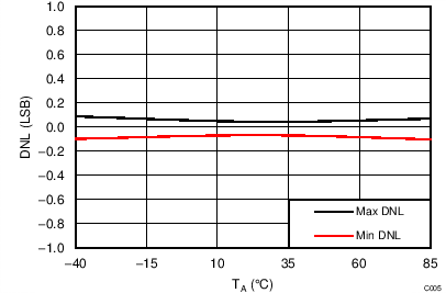
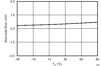
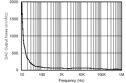
at AVCC = 12 V, AVSS = –12 V, DVDD = 3.3 V, AGND = DGND = REFGND[1,2] = 0 V, REF1 = REF2 = 2.5 V (specifications exclude any reference contributions), no load on DACs, and TA = 25°C (unless otherwise noted)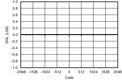
6.10 Typical Characteristics: Toggle Mode
at AVCC = 12 V, AVSS = –12 V, DVDD = 3.3 V, AGND = DGND = REFGND[1,2] = 0 V, REF1 = REF2 = 2.5 V (specifications exclude any reference contributions), no load on DACs, and TA = 25°C (unless otherwise noted)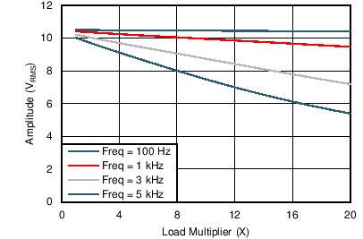
| 1x load: R(SERIES) = 100 kΩ, CLOAD = 50 pF |
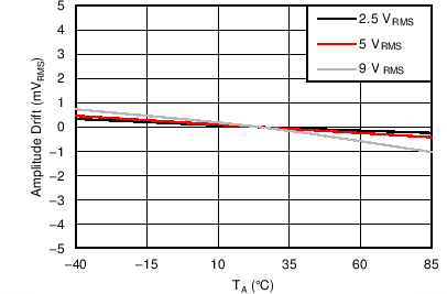
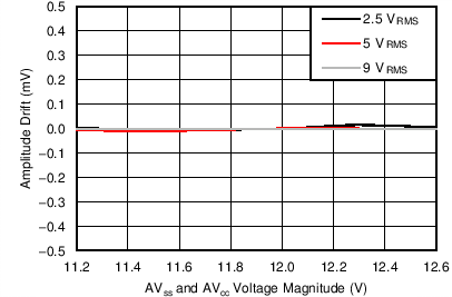
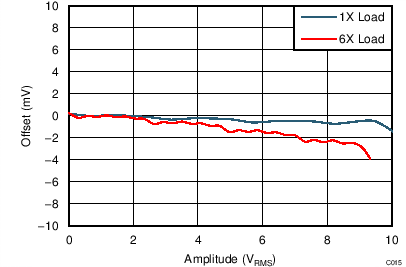
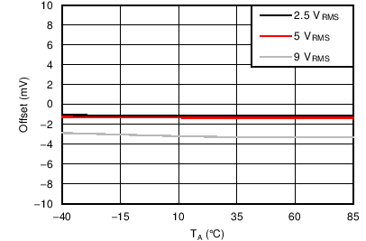
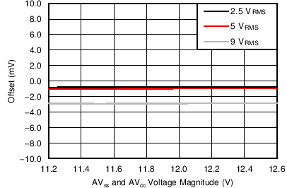
6.11 Typical Characteristics, General
at AVCC = 12 V, AVSS = –12 V, DVDD = 3.3 V, AGND = DGND = REFGND[1,2] = 0 V, REF1 = REF2 = 2.5 V (specifications exclude any reference contributions), no load on DACs, and TA = 25°C (unless otherwise noted)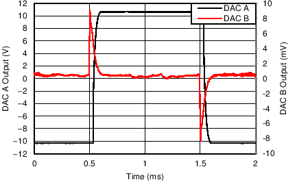
| DAC A: square-wave output, freq = 1 kHz, full-scale amplitude | ||
| DAC B: zero-code inputs |
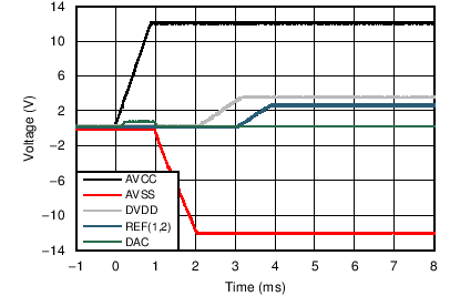
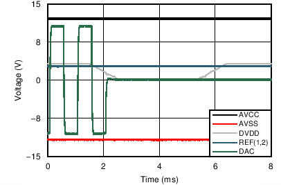
| 6x load: R(SERIES) = 17 kΩ, CLOAD = 300 pF | ||
| Square-wave output: freq = 1 kHz, full-scale amplitude |
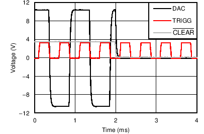
| 6x load: R(SERIES) = 17 kΩ, CLOAD = 300 pF | ||
| Square-wave output: freq = 1 kHz, full-scale amplitude |
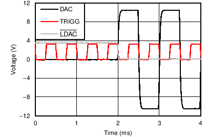
| 6x load: R(SERIES) = 17 kΩ, CLOAD = 300 pF | ||
| Square-wave output: freq = 1 kHz, full-scale amplitude |
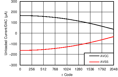
| No DAC load, DVDD = 3.3 V | ||
| Square-wave output: freq = 3 kHz |
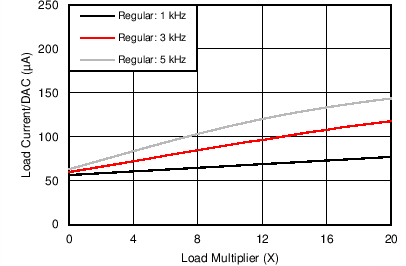
| 1x load: R(SERIES) = 100 kΩ, CLOAD = 50 pF, DVDD = 3.3 V | ||
| Square-wave output, full-scale amplitude |
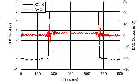
| All DACs with zero-code inputs | ||
| SCLK frequency = 1 MHz |
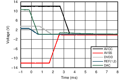
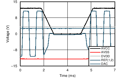
| 6x load: R(SERIES) = 17 kΩ, CLOAD = 300 pF | ||
| Square-wave output: freq = 1 kHz, full-scale amplitude |
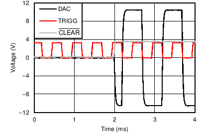
| 6x load: R(SERIES) = 17 kΩ, CLOAD = 300 pF | ||
| Square-wave output: freq = 1 kHz, full-scale amplitude |
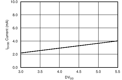
| No DAC load | ||
| Square-wave output: freq = 3 kHz, full-scale amplitude |
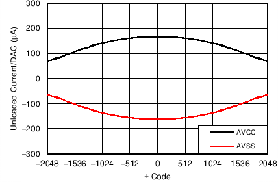
| No DAC load, DC output, DVDD = 3.3 V | ||
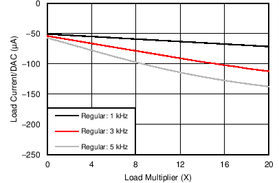
| 1x load: R(SERIES) = 100 kΩ, CLOAD = 50 pF, DVDD = 3.3 V | ||
| Square-wave output, full-scale amplitude |