ZHCSEG7A December 2015 – January 2016 DAC60096
PRODUCTION DATA.
- 1 特性
- 2 应用
- 3 说明
- 4 修订历史记录
- 5 Pin Configuration and Functions
-
6 Specifications
- 6.1 Absolute Maximum Ratings
- 6.2 ESD Ratings
- 6.3 Recommended Operating Conditions
- 6.4 Thermal Information
- 6.5 Electrical Characteristics: DAC DC
- 6.6 Electrical Characteristics: Square-Wave Output
- 6.7 Electrical Characteristics: General
- 6.8 Timing Requirements
- 6.9 Typical Characteristics: DC Mode
- 6.10 Typical Characteristics: Toggle Mode
- 6.11 Typical Characteristics, General
-
7 Detailed Description
- 7.1 Overview
- 7.2 Functional Block Diagram
- 7.3 Feature Description
- 7.4 Device Functional Modes
- 7.5 Programming
- 7.6
Register Maps
- 7.6.1 8.5.1 BUFA Register (address = 0x0) [reset = 0x0000]
- 7.6.2 BUFB Register (address = 0x1) [reset = 0x0000]
- 7.6.3 CON Register (address = 0x4) [reset = 0x0555]
- 7.6.4 CRC Register (address = 0x5) [reset = 0xFFF]
- 7.6.5 PTR Register (address = 0x6) [reset = 0x0000]
- 7.6.6 SWR Register (address = 0x7) [reset = 0x0000]
- 7.6.7 PWRM Register (address = 0x6) [reset = 0xCAFE]
- 7.6.8 SDIV Register (address = 0x9) [reset = 0x0000]
- 8 Application and Implementation
- 9 Power Supply Recommendations
- 10Layout
- 11器件和文档支持
- 12机械、封装和可订购信息
8 Application and Implementation
NOTE
Information in the following applications sections is not part of the TI component specification, and TI does not warrant its accuracy or completeness. TI’s customers are responsible for determining suitability of components for their purposes. Customers should validate and test their design implementation to confirm system functionality.
8.1 Application Information
The DAC60096 is a low-power, 96-channel, 12-bit, digital-to-analog converter (DAC). The device provides unbuffered bipolar voltage outputs up to ±10.5 V.
This device is suitable for many applications involving multichannel bipolar DACs. Such applications include multichannel variable optical attenuators, MEMS mirror control, and ATE level drivers.
8.2 Typical Application
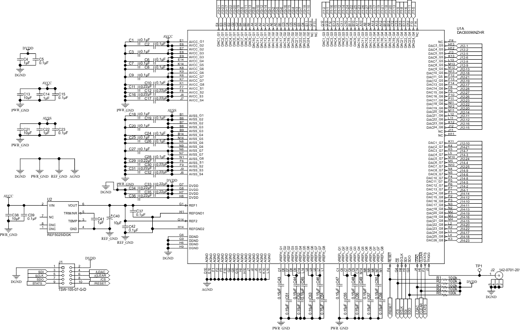
An example schematic incorporating the DAC60096 device is shown in Figure 49.
 Figure 49. Example Schematic
8.2.1 Design Requirements
Figure 49 uses the parameters shown in Table 12.
Table 12. Design Parameters
| PARAMETER | VALUE |
|---|---|
| AVCC | 12 V |
| DVDD | 5 V |
| AVSS | –12 V |
| REF1 | 2.5 V |
| REF2 | 2.5 V |
8.2.2 Detailed Design Procedure
The following sections display components and applications that may facilitate the design process.
8.2.2.1 Power-Supply Bypassing
For accurate, high-resolution performance, all power supply pins should be bypassed to ground with low ESR ceramic bypass capacitors. For additional noise filtering, use a 10-µF capacitor in parallel with a 0.1-µF capacitor.
8.2.2.2 Reference Input
The internal reference buffers of the DAC60096 device require an external 2.5-V reference voltage source, which can be driven externally through a precision voltage source or generated from a high precision voltage IC. One such integrated circuit is the REF5025, which is a low-noise, low-drift, high precision voltage reference. The basic connections are listed in Figure 50. A supply bypass capacitor ranging between 1 µF to 10 µF is recommended. A 1-µF to 50-µF output capacitor must be connected from VOUT to GND. The ESR value of the output capacitor must be less than or equal to 1.5 Ω to ensure output stability. To help minimize noise, an additional 1-µF capacitor is connected from TRIM/NR to GND.
8.2.2.3 TRIGG/Signal Conditioning
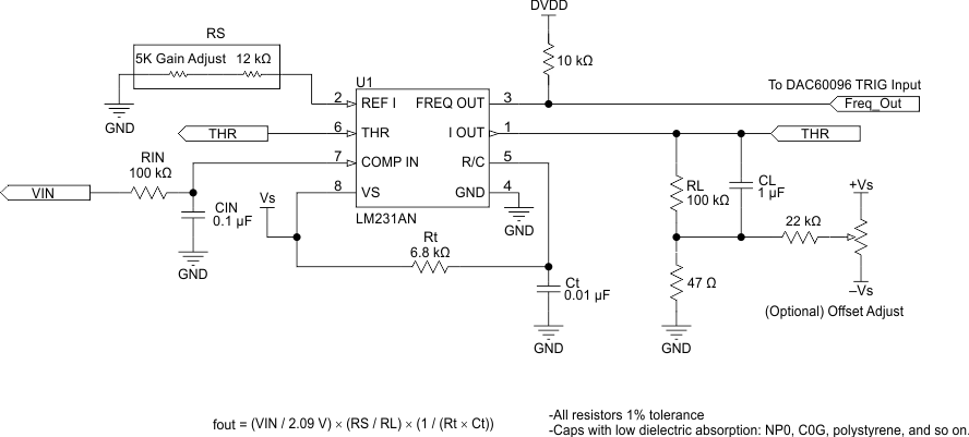
The TRIGG input signal provides the square waveform required for the DAC60096 device to operate as a square-wave generator. The DAC registers are prepared for square wave operation on a TRIGG rising edge and the outputs toggle on the falling edge. The Timing Requirements table specifies the timing parameters required for proper operation.
The TRIGG input signal can be supplied from a waveform generator or voltage-to-frequency converter. An example device with schematic is provided in Figure 51. The device highlighted is the LM231, a precision voltage-to-frequency converter with wide range of full-scale frequency (1 Hz to 100 kHz). In Figure 51 the device is configured to display 0.05% linearity over an output frequency range of 10 Hz to 4 kHz with and input range of 25 mV to 12.5 V. For more information, refer to the Typical Applications section of the LM231 datasheet (SNOSBI2).
 Figure 51. External Precision Voltage-to-Frequency Converter for TRIGG Signal
8.2.2.4 External Amplifier Selection
The outputs of the DAC60096 are unbuffered. The output impedance is specified as 41 kΩ. In applications requiring an external buffer, the selected amplifier should exhibit both low-offset voltage and input bias current. The input bias current of the amplifier creates a potential across the DAC output impedance. This voltage error is equivalent to the input bias current multiplied by the DAC output impedance value. For fast settling, the slew rate of the operational amplifier should not impede the settling time of the DAC. Output impedance of the DAC is constant and code-independent, but in order to minimize gain errors the input impedance of the output amplifier should be as high as possible. Additionally, the amplifier adds another time constant, which increases the settling time response of the system. A higher 3-dB bandwidth amplifier effectively shortens the settling time, and additionally increases the bandwidth of the system.
8.2.2.5 Unbuffered Settling Response
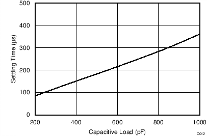
For applications that use the unbuffered output, the typical settling response for different capacitive loads is displayed in Figure 53.
8.2.3 Application Curves
