ZHCSH59C August   2017  – January 2019 DAC60504 , DAC70504 , DAC80504

PRODUCTION DATA.  

  1. 特性
  2. 应用
  3. 说明
    1.     Device Images
      1.      简化方框图
  4. 修订历史记录
  5. Device Comparison Table
  6. Pin Configuration and Functions
    1.     Pin Functions
  7. Specifications
    1. 7.1 Absolute Maximum Ratings
    2. 7.2 ESD Ratings
    3. 7.3 Recommended Operating Conditions
    4. 7.4 Thermal Information
    5. 7.5 Electrical Characteristics
    6. 7.6 Typical Characteristics
  8. Detailed Description
    1. 8.1 Overview
    2. 8.2 Functional Block Diagram
    3. 8.3 Feature Description
      1. 8.3.1 Digital-to-Analog Converter (DAC)
        1. 8.3.1.1 DAC Transfer Function
        2. 8.3.1.2 Output Amplifiers
        3. 8.3.1.3 DAC Register Structure
          1. 8.3.1.3.1 DAC Register Synchronous and Asynchronous Updates
          2. 8.3.1.3.2 Broadcast DAC Register
      2. 8.3.2 Internal Reference
        1. 8.3.2.1 Reference Divider
        2. 8.3.2.2 Solder Heat Reflow
      3. 8.3.3 Device Reset Options
        1. 8.3.3.1 Power-on-Reset (POR)
        2. 8.3.3.2 Software Reset
    4. 8.4 Device Functional Modes
      1. 8.4.1 Stand-Alone Operation
      2. 8.4.2 Daisy-Chain Operation
      3. 8.4.3 Frame Error Checking
      4. 8.4.4 Power-Down Mode
    5. 8.5 Programming
    6. 8.6 Register Map
      1. 8.6.1 NOP Register (address = 0x00) [reset = 0x0000]
        1. Table 9. NOP Register Field Descriptions
      2. 8.6.2 DEVICE ID Register (address = 0x01) [reset = 0x---]
        1. Table 10. DEVICE ID Field Descriptions
      3. 8.6.3 SYNC Register (address = 0x2) [reset = 0xFF00]
        1. Table 11. SYNC Register Field Descriptions
      4. 8.6.4 CONFIG Register (address = 0x3) [reset = 0x0000]
        1. Table 12. CONFIG Register Field Descriptions
      5. 8.6.5 GAIN Register (address = 0x04) [reset = 0x---]
        1. Table 13. GAIN Register Field Descriptions
      6. 8.6.6 TRIGGER Register (address = 0x05) [reset = 0x0000]
        1. Table 14. TRIGGER Register Field Descriptions
      7. 8.6.7 BRDCAST Register (address = 0x6) [reset = 0x0000]
        1. Table 15. BRDCAST Register Field Descriptions
      8. 8.6.8 STATUS Register (address = 0x7) [reset = 0x0000]
        1. Table 16. STATUS Register Field Descriptions
      9. 8.6.9 DACx Register (address = 0x8 to 0xF) [reset = 0x0000 or 0x8000]
        1. Table 17. DACx Register Field Descriptions
  9. Application and Implementation
    1. 9.1 Application Information
      1. 9.1.1 Interfacing to a Microcontroller
      2. 9.1.2 Programmable Current Source Circuit
    2. 9.2 Typical Application
      1. 9.2.1 Design Requirements
      2. 9.2.2 Detailed Design Procedure
      3. 9.2.3 Application Curve
  10. 10Power Supply Recommendations
  11. 11Layout
    1. 11.1 Layout Guidelines
    2. 11.2 Layout Example
  12. 12器件和文档支持
    1. 12.1 文档支持
      1. 12.1.1 相关文档
    2. 12.2 相关链接
    3. 12.3 接收文档更新通知
    4. 12.4 社区资源
    5. 12.5 商标
    6. 12.6 静电放电警告
    7. 12.7 术语表
  13. 13机械、封装和可订购信息

封装选项

机械数据 (封装 | 引脚)
散热焊盘机械数据 (封装 | 引脚)
订购信息

Programming

The DACx0504 is controlled through a flexible four-wire serial interface that is compatible with SPI type interfaces used on many microcontrollers and DSP controllers. The interface provides read and write access to all DACx0504 registers and can also be configured to daisy-chain multiple devices for write operations. The DACx0504 incorporates an optional error checking mode to validate SPI data communication integrity in noisy environments. Table 7 shows the SPI timing requirements. Figure 62 and Figure 63 show the SPI write and read timing diagrams, respectively. Figure 64 shows the digital logic timing diagram.

Table 7. Programming Timing Requirements(1)

VIO = 1.7 V to 2.7 V VIO = 2.7 V to 5.5 V UNIT
MIN NOM MAX MIN NOM MAX
SERIAL INTERFACE – WRITE OPERATION
fSCLK SCLK frequency 50 50 MHz
tSCLKHIGH SCLK high time 9 9 ns
tSCLKLOW SCLK low time 9 9 ns
tSDIS SDI setup 5 5 ns
tSDIH SDI hold 10 10 ns
tCSS CS to SCLK falling edge setup 13 13 ns
tCSH SCLK falling edge to CS rising edge 10 10 ns
tCSHIGH CS high time 15 15 ns
tCSIGNORE SCLK falling edge to CS ignore 7 7 ns
SERIAL INTERFACE – READ AND DAISY CHAIN OPERATION, FSDO = 0
fSCLK SCLK frequency 12 18 MHz
tSCLKHIGH SCLK high time 35 25 ns
tSCLKLOW SCLK low time 35 25 ns
tSDIS SDI setup 5 5 ns
tSDIH SDI hold 10 10 ns
tCSS CS to SCLK falling edge setup 32 20 ns
tCSH SCLK falling edge to CS rising edge 10 10 ns
tCSHIGH CS high time 15 15 ns
tSDODLY SDO output delay from SCLK rising edge 3.5 33.5 3.5 23 ns
tSDODZ SDO driven to tri-state 0 30 0 25 ns
tCSIGNORE SCLK falling edge to CS ignore 7 7 ns
SERIAL INTERFACE – READ AND DAISY CHAIN OPERATION, FSDO = 1
fSCLK SCLK frequency 20 25 MHz
tSCLKHIGH SCLK high time 22 18 ns
tSCLKLOW SCLK low time 22 18 ns
tSDIS SDI setup 5 5 ns
tSDIH SDI hold 10 10 ns
tCSS CS to SCLK falling edge setup 32 20 ns
tCSH SCLK falling edge to CS rising edge 10 10 ns
tCSHIGH CS high time 15 15 ns
tSDODLY SDO output delay from SCLK falling edge 3.5 45 3.5 32 ns
tSDODZ SDO driven to tri-state 0 30 0 25 ns
tCSIGNORE SCLK falling edge to CS ignore 7 7 ns
DIGITAL LOGIC
tRSTDLYPOR POR reset delay 170 250 170 250 µs
tDACWAIT Sequential DAC output updates 1 1 µs
tLDACS LDAC setup 0 0 ns
tLDACH LDAC hold 5 5 ns
All input signals are specified at tR = tF = 1 ns/V (10% to 90% of VIO), timed from a voltage level of (VIL + VIH) / 2, VDD = 2.7 V to 5.5 V, VIO = 1.7 V to 5.5 V, VREFIN = 1.25 V to 5.5 V, SDO loaded with 20 pF, and TA = –40°C to +125°C (unless otherwise noted)
DAC80504 DAC70504 DAC60504 dac80504-serial-interface-write-timing.gifFigure 62. Serial Interface Write Timing Diagram
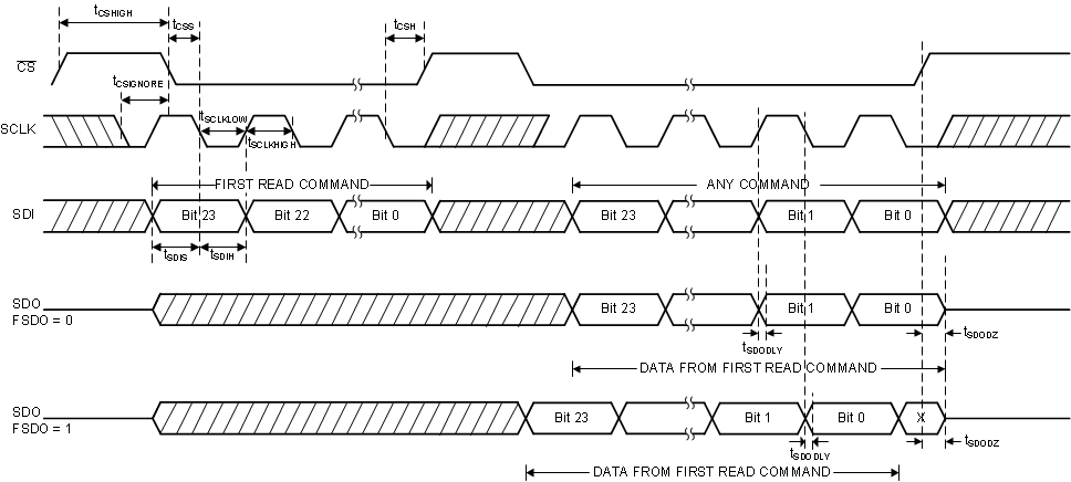
DAC80504 DAC70504 DAC60504 dac80504-serial-interface-read-timing.gifFigure 63. Serial Interface Read Timing Diagram
DAC80504 DAC70504 DAC60504 dac80504-digital-logic-timing-diagram.gifFigure 64. Digital Logic Timing Diagram