ZHCSH59C August   2017  – January 2019 DAC60504 , DAC70504 , DAC80504

PRODUCTION DATA.  

  1. 特性
  2. 应用
  3. 说明
    1.     Device Images
      1.      简化方框图
  4. 修订历史记录
  5. Device Comparison Table
  6. Pin Configuration and Functions
    1.     Pin Functions
  7. Specifications
    1. 7.1 Absolute Maximum Ratings
    2. 7.2 ESD Ratings
    3. 7.3 Recommended Operating Conditions
    4. 7.4 Thermal Information
    5. 7.5 Electrical Characteristics
    6. 7.6 Typical Characteristics
  8. Detailed Description
    1. 8.1 Overview
    2. 8.2 Functional Block Diagram
    3. 8.3 Feature Description
      1. 8.3.1 Digital-to-Analog Converter (DAC)
        1. 8.3.1.1 DAC Transfer Function
        2. 8.3.1.2 Output Amplifiers
        3. 8.3.1.3 DAC Register Structure
          1. 8.3.1.3.1 DAC Register Synchronous and Asynchronous Updates
          2. 8.3.1.3.2 Broadcast DAC Register
      2. 8.3.2 Internal Reference
        1. 8.3.2.1 Reference Divider
        2. 8.3.2.2 Solder Heat Reflow
      3. 8.3.3 Device Reset Options
        1. 8.3.3.1 Power-on-Reset (POR)
        2. 8.3.3.2 Software Reset
    4. 8.4 Device Functional Modes
      1. 8.4.1 Stand-Alone Operation
      2. 8.4.2 Daisy-Chain Operation
      3. 8.4.3 Frame Error Checking
      4. 8.4.4 Power-Down Mode
    5. 8.5 Programming
    6. 8.6 Register Map
      1. 8.6.1 NOP Register (address = 0x00) [reset = 0x0000]
        1. Table 9. NOP Register Field Descriptions
      2. 8.6.2 DEVICE ID Register (address = 0x01) [reset = 0x---]
        1. Table 10. DEVICE ID Field Descriptions
      3. 8.6.3 SYNC Register (address = 0x2) [reset = 0xFF00]
        1. Table 11. SYNC Register Field Descriptions
      4. 8.6.4 CONFIG Register (address = 0x3) [reset = 0x0000]
        1. Table 12. CONFIG Register Field Descriptions
      5. 8.6.5 GAIN Register (address = 0x04) [reset = 0x---]
        1. Table 13. GAIN Register Field Descriptions
      6. 8.6.6 TRIGGER Register (address = 0x05) [reset = 0x0000]
        1. Table 14. TRIGGER Register Field Descriptions
      7. 8.6.7 BRDCAST Register (address = 0x6) [reset = 0x0000]
        1. Table 15. BRDCAST Register Field Descriptions
      8. 8.6.8 STATUS Register (address = 0x7) [reset = 0x0000]
        1. Table 16. STATUS Register Field Descriptions
      9. 8.6.9 DACx Register (address = 0x8 to 0xF) [reset = 0x0000 or 0x8000]
        1. Table 17. DACx Register Field Descriptions
  9. Application and Implementation
    1. 9.1 Application Information
      1. 9.1.1 Interfacing to a Microcontroller
      2. 9.1.2 Programmable Current Source Circuit
    2. 9.2 Typical Application
      1. 9.2.1 Design Requirements
      2. 9.2.2 Detailed Design Procedure
      3. 9.2.3 Application Curve
  10. 10Power Supply Recommendations
  11. 11Layout
    1. 11.1 Layout Guidelines
    2. 11.2 Layout Example
  12. 12器件和文档支持
    1. 12.1 文档支持
      1. 12.1.1 相关文档
    2. 12.2 相关链接
    3. 12.3 接收文档更新通知
    4. 12.4 社区资源
    5. 12.5 商标
    6. 12.6 静电放电警告
    7. 12.7 术语表
  13. 13机械、封装和可订购信息

封装选项

机械数据 (封装 | 引脚)
散热焊盘机械数据 (封装 | 引脚)
订购信息

Typical Application

The DACx0504 is designed for single-supply operation; however, a bipolar output is also possible using the circuit shown in Figure 76.
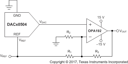
DAC80504 DAC70504 DAC60504 dac80504-bipolar-output-operation.gifFigure 76. Bipolar Operation Using the DACx0504