at TA = 25°C,
VDD = 5.5 V, Internal reference = 2.5 V, REF-DIV = 0 and BUFF-GAIN = 1, and DAC
outputs unloaded (unless otherwise noted)
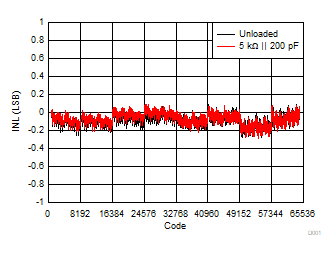
 Figure 7-3 Integral Linearity Error vs Digital Input Code
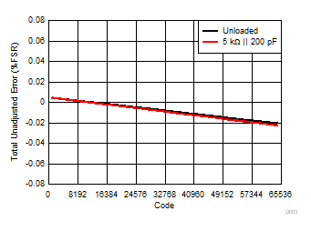
 Figure 7-5 Total Unadjusted Error vs Digital Input Code
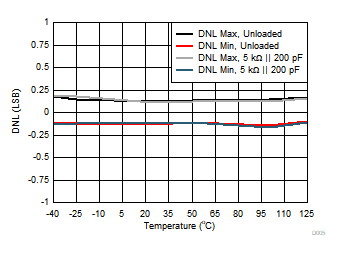
 Figure 7-7 Differential Linearity Error vs Temperature
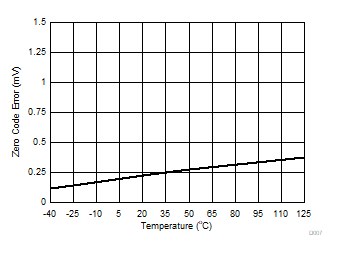
 Figure 7-9 Zero Code Error vs Temperature
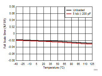
 Figure 7-11 Full Scale Error vs Temperature
| REF-DIV = 0 and BUFF-GAIN = 0 |
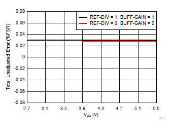
 Figure 7-15 Total
Unadjusted Error vs Supply Voltage
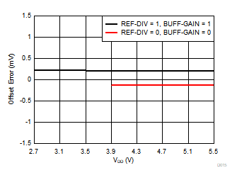
 Figure 7-17 Offset Error vs Supply Voltage
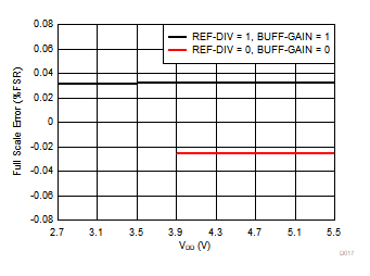
 Figure 7-19 Full
Scale Error vs Supply Voltage
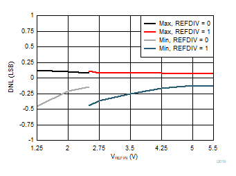
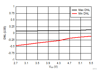
 Figure 7-21 Differential Linearity Error vs Reference Voltage
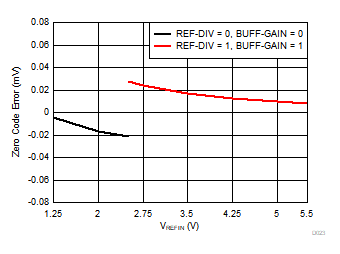
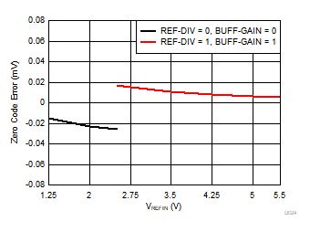
 Figure 7-23 Zero
Code Error vs Reference Voltage
 Figure 7-25 Gain
Error vs Reference Voltage
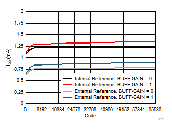
 Figure 7-27 Supply Current vs Digital Input Code
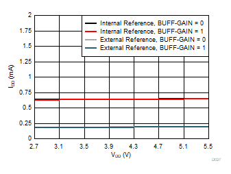
 Figure 7-29 Supply Current vs Supply Voltage
| External reference = 2.5 V, REF-DIV = 1 and BUFF-GAIN =
0 |
Figure 7-31 Power
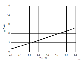
Down Current vs Supply Voltage
| REF-DIV = 0 and BUFF-GAIN = 0 |
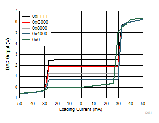
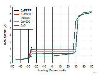
Figure 7-33 Source and Sink Capability
| REF-DIV = 1 and BUFF-GAIN = 0 |
| |
Figure 7-35 Source and Sink Capability
| DAC
code transition from midscale to midscale – 1
LSB, |
| REF-DIV = 0 and BUFF-GAIN = 0 |
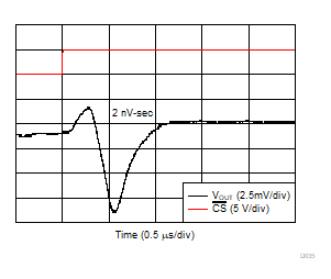
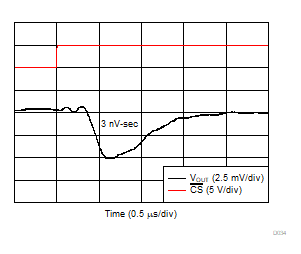
Figure 7-37 Glitch Impulse, Falling Edge, 1‑LSB Step
| REF-DIV = 0 and BUFF-GAIN = 0 |
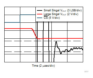
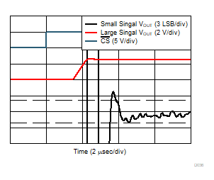
Figure 7-39 Full-Scale Settling Time, Falling Edge
| REF-DIV = 0 and BUFF-GAIN = 0 |
| |
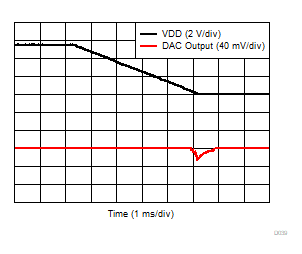
Figure 7-41 Power-off Glitch
| fo = 1 kHz, fs = 400 kHz,
includes 7 harmonics, |
| measurement bandwidth = 20 kHz, external reference =
2.5 V, |
| REF-DIV = 0 and BUFF-GAIN = 0 |
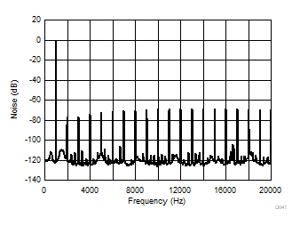
Figure 7-43 DAC
Output THD+N vs Frequency
| DAC
code at midscale, external reference = 2.5 V, |
| REF-DIV = 0 and BUFF-GAIN = 0 |
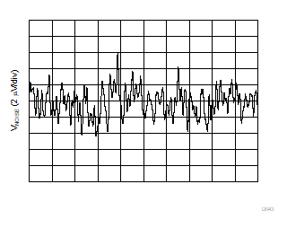
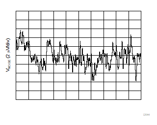
Figure 7-45 DAC
Output Noise 0.1 Hz to 10 Hz
| DAC
code at midscale, external reference = 2.5 V, |
| SCLK
= 1 MHz, REF-DIV = 0 and BUFF-GAIN = 0 |
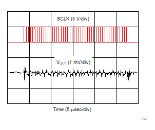
Figure 7-47 Clock
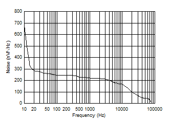
Feedthrough Figure 7-49 Internal Reference Voltage vs Supply Voltage
 Figure 7-51 Internal Reference Noise Density vs Frequency
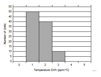
 Figure 7-53 Internal Reference Temperature Drift Histogram
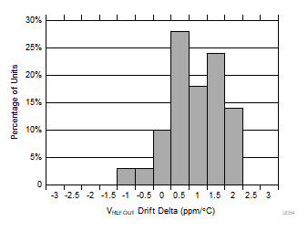
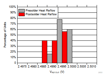
 Figure 7-55 Internal Reference
Temperature Drift (Pre- and Post-Solder) Histogram
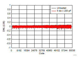
 Figure 7-4 Differential Linearity Error vs Digital Input Code
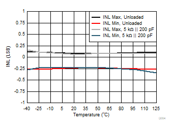
 Figure 7-6 Integral Linearity Error vs Temperature
 Figure 7-8 Total Unadjusted Error vs Temperature
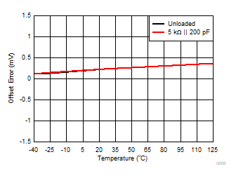
 Figure 7-10 Offset Error vs Temperature
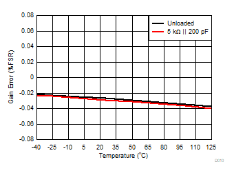
 Figure 7-12 Gain Error vs Temperature
| REF-DIV = 0 and BUFF-GAIN = 0 |
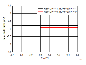
 Figure 7-16 Zero
Code Error vs Supply Voltage
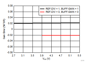
 Figure 7-18 Gain
Error vs Supply Voltage
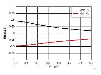
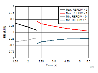
 Figure 7-20 Integral Linearity Error vs Reference Voltage
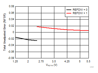
 Figure 7-22 Total
Unadjusted Error vs Reference Voltage
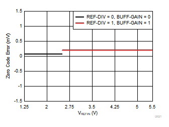
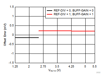
 Figure 7-24 Offset Error vs Reference Voltage
 Figure 7-26 Full
Scale Error vs Reference Voltage
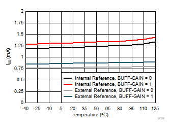
 Figure 7-28 Supply Current vs Temperature
| REF-DIV = 0 and BUFF-GAIN = 0 |
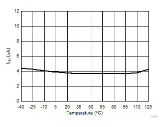
Figure 7-30 Power
Down Current vs Temperature
| External reference = 2.5 V |
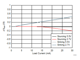
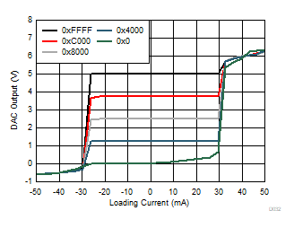
Figure 7-32 Headroom and Footroom vs Load Current
| REF-DIV = 0 and BUFF-GAIN = 1 |
Figure 7-34 Source and Sink Capability
| DAC
code transition from midscale – 1 to midscale
LSB, |
| REF-DIV = 0 and BUFF-GAIN = 0 |
Figure 7-36 Glitch Impulse, Rising Edge, 1‑LSB Step
| REF-DIV = 0 and BUFF-GAIN = 0 |
| |
Figure 7-38 Full-Scale Settling Time, Rising Edge
| REF-DIV = 0 and BUFF-GAIN = 0 |
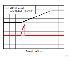
Figure 7-40 Power-on Glitch
| DAC
code at midscale, VDD = 5.0 V + 0.2
VPP, |
| REF-DIV = 0 and BUFF-GAIN = 0 |
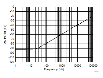
Figure 7-42 DAC
Output AC PSRR vs Frequency
| Gain
= 1X (REF-DIV = 1 and BUFF-GAIN = 1), |
| external reference = 2.5 V, |
| REF-DIV = 0 and BUFF-GAIN = 0 |
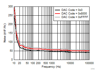
Figure 7-44 DAC
Output Noise Spectral Density
| DAC
code at midscale, internal reference = 2.5 V, |
| REF-DIV = 0 and BUFF-GAIN = 0 |
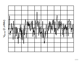
Figure 7-46 DAC
Output Noise 0.1 Hz to 10 Hz Figure 7-48 Internal Reference Voltage vs Temperature
 Figure 7-50 Internal Reference Voltage vs Time
 Figure 7-52 Internal Reference Noise, 0.1 Hz to 10 Hz
 Figure 7-54 Internal Reference Initial Accuracy (Pre- and Post-Solder)
Histogram