ZHCSKJ2A November 2019 – April 2020 DAC60502 , DAC70502 , DAC80502
PRODUCTION DATA.
- 1 特性
- 2 应用
- 3 说明
- 4 修订历史记录
- 5 Device Comparison Table
- 6 Pin Configuration and Functions
-
7 Specifications
- 7.1 Absolute Maximum Ratings
- 7.2 ESD Ratings
- 7.3 Recommended Operating Conditions
- 7.4 Thermal Information
- 7.5 Electrical Characteristics
- 7.6 Timing Requirements : SPI Mode
- 7.7 Timing Requirements : I2C Standard Mode
- 7.8 Timing Requirements : I2C Fast Mode
- 7.9 Timing Requirements : I2C Fast-Mode Plus
- 7.10 Typical Characteristics
-
8 Detailed Description
- 8.1 Overview
- 8.2 Functional Block Diagram
- 8.3 Feature Description
- 8.4 Device Functional Modes
- 8.5 Programming
- 8.6
Register Maps
- 8.6.1
Registers
- 8.6.1.1 NOOP Register (offset = 0h) [reset = 0000h]
- 8.6.1.2 DEVID Register (offset = 1h) [reset = 0214h for DAC80502, 1214h for DAC70502, 2214h for DAC60502]
- 8.6.1.3 SYNC Register (offset = 2h) [reset = 0300h]
- 8.6.1.4 CONFIG Register (offset = 3h) [reset = 0000h]
- 8.6.1.5 GAIN Register (offset = 4h) [reset = 0003h]
- 8.6.1.6 TRIGGER Register (offset = 5h) [reset = 0000h]
- 8.6.1.7 BRDCAST Register (offset = 6h) [reset = 0000h for RSTSEL = 0, or reset = 8000h for RSTSEL = 1]
- 8.6.1.8 STATUS Register (offset = 7h) [reset = 0000h]
- 8.6.1.9 DAC-n Register (offset = 8h–9h) [reset = 0000h for RSTSEL = 0, or reset = 8000h for RSTSEL = 1]
- 8.6.1
Registers
- 9 Application and Implementation
- 10Power Supply Recommendations
- 11Layout
- 12器件和文档支持
- 13机械、封装和可订购信息
8.3.3 Power-On Reset (POR)
The DACx0502 family of devices includes a power-on reset function that controls the output voltage at power up. After the VDD supply has been established, a POR event is issued. The POR causes all registers to initialize to default values, and communication with the device is valid only after a 250-µs, power-on-reset delay. The default value for all DACs is zero code if RSTSEL = 0, and midscale code if RSTSEL = 1. Each DAC channel remains at the power-up voltage until a valid command is written to a channel.
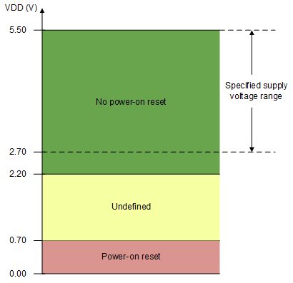
When the device powers up, a POR circuit sets the device to the default mode. The POR circuit requires specific VDD levels, as indicated in Figure 57, in order to make sure that the internal capacitors discharge and reset the device on power up. In order to make sure that a POR occurs, VDD must be less than 0.7 V for at least 1 ms. When VDD drops to less than 2.2 V but remains greater than 0.7 V (shown as the undefined region), the device may or may not reset under all specified temperature and power-supply conditions. In this case, initiate a POR. When VDD remains greater than 2.2 V, a POR does not occur.
 Figure 57. Threshold Levels for the VDD POR Circuit