ZHCSH64D June   2017  – August 2018 DAC60508 , DAC70508 , DAC80508

PRODUCTION DATA.  

  1. 特性
  2. 应用
  3. 说明
    1.     Device Images
      1.      简化方框图
  4. 修订历史记录
  5. Device Comparison Table
  6. Pin Configuration and Functions
    1.     Pin Functions
  7. Specifications
    1. 7.1 Absolute Maximum Ratings
    2. 7.2 ESD Ratings
    3. 7.3 Recommended Operating Conditions
    4. 7.4 Thermal Information
    5. 7.5 Electrical Characteristics
    6. 7.6 Typical Characteristics
  8. Detailed Description
    1. 8.1 Overview
    2. 8.2 Functional Block Diagram
    3. 8.3 Feature Description
      1. 8.3.1 Digital-to-Analog Converter (DAC) Architecture
        1. 8.3.1.1 DAC Transfer Function
        2. 8.3.1.2 Output Amplifiers
        3. 8.3.1.3 DAC Register Structure
          1. 8.3.1.3.1 DAC Register Synchronous and Asynchronous Updates
          2. 8.3.1.3.2 Broadcast DAC Register
          3. 8.3.1.3.3 CLEAR Operation (DACx0508C only)
      2. 8.3.2 Internal Reference
        1. 8.3.2.1 Reference Divider
        2. 8.3.2.2 Solder Heat Reflow
      3. 8.3.3 Device Reset Options
        1. 8.3.3.1 Power-on-Reset (POR)
        2. 8.3.3.2 Software Reset
    4. 8.4 Device Functional Modes
      1. 8.4.1 Stand-Alone Operation
      2. 8.4.2 Daisy-Chain Operation
      3. 8.4.3 Frame Error Checking
      4. 8.4.4 Power-Down Mode
    5. 8.5 Programming
    6. 8.6 Register Map
      1. 8.6.1 NOP Register (address = 0x00) [reset = 0x0000]
        1. Table 9. NOP Register Field Descriptions
      2. 8.6.2 DEVICE ID Register (address = 0x01) [reset = 0x---]
        1. Table 10. DEVICE ID Field Descriptions
      3. 8.6.3 SYNC Register (address = 0x2) [reset = 0xFF00]
        1. Table 11. SYNC Register Field Descriptions
      4. 8.6.4 CONFIG Register (address = 0x3) [reset = 0x0000]
        1. Table 12. CONFIG Register Field Descriptions
      5. 8.6.5 GAIN Register (address = 0x04) [reset = 0x---]
        1. Table 13. GAIN Register Field Descriptions
      6. 8.6.6 TRIGGER Register (address = 0x05) [reset = 0x0000]
        1. Table 14. TRIGGER Register Field Descriptions
      7. 8.6.7 BRDCAST Register (address = 0x6) [reset = 0x0000]
        1. Table 15. BRDCAST Register Field Descriptions
      8. 8.6.8 STATUS Register (address = 0x7) [reset = 0x0000]
        1. Table 16. STATUS Register Field Descriptions
      9. 8.6.9 DACx Register (address = 0x8 to 0xF) [reset = 0x0000 or 0x8000]
        1. Table 17. DACx Register Field Descriptions
  9. Application and Implementation
    1. 9.1 Application Information
      1. 9.1.1 Interfacing to Microcontroller
      2. 9.1.2 Programmable Current Source Circuit
    2. 9.2 Typical Application
      1. 9.2.1 Design Requirements
      2. 9.2.2 Detailed Design Procedure
      3. 9.2.3 Application Curve
  10. 10Power Supply Recommendations
  11. 11Layout
    1. 11.1 Layout Guidelines
    2. 11.2 Layout Examples
  12. 12器件和文档支持
    1. 12.1 相关链接
    2. 12.2 接收文档更新通知
    3. 12.3 社区资源
    4. 12.4 商标
    5. 12.5 静电放电警告
    6. 12.6 术语表
  13. 13机械、封装和可订购信息

封装选项

机械数据 (封装 | 引脚)
散热焊盘机械数据 (封装 | 引脚)
订购信息

Typical Characteristics

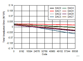
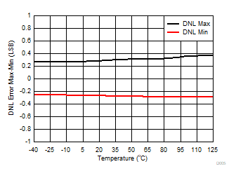
At TA = 25°C, VDD = 5.5 V, Internal Reference = 2.5 V, Gain = 2, DAC outputs unloaded, unless otherwise noted.
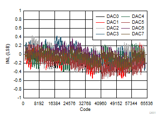
DAC80508 DAC70508 DAC60508 D001.gif
Figure 1. Integral Linearity Error vs Digital Input Code
DAC80508 DAC70508 DAC60508 D003.gif
Figure 3. Total Unadjusted Error vs Digital Input Code
DAC80508 DAC70508 DAC60508 D005.gif
Figure 5. Differential Linearity Error vs Temperature
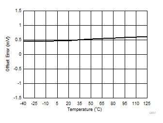
DAC80508 DAC70508 DAC60508 D007.gif
Figure 7. Offset Error vs Temperature
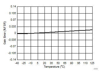
DAC80508 DAC70508 DAC60508 D009.gif
Figure 9. Gain Error vs Temperature
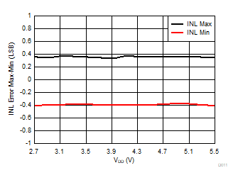
DAC80508 DAC70508 DAC60508 D011.gif
Gain = 1
Figure 11. Integral Linearity Error vs Supply Voltage
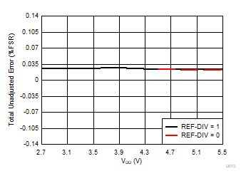
DAC80508 DAC70508 DAC60508 D013.gif
Gain = 1
Figure 13. Total Unadjusted Error vs Supply Voltage
DAC80508 DAC70508 DAC60508 D015.gif
Gain = 1
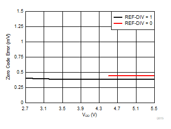
Figure 15. Zero Code Error vs Supply Voltage
DAC80508 DAC70508 DAC60508 D017.gif
Gain = 1
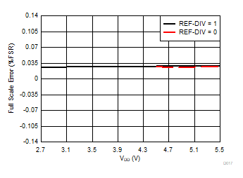
Figure 17. Full Scale Error vs Supply Voltage
DAC80508 DAC70508 DAC60508 D019_SLASEL1.gif
Gain = 1
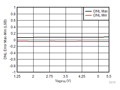
Figure 19. Differential Linearity Error vs Reference Voltage
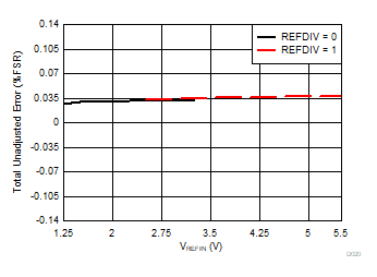
DAC80508 DAC70508 DAC60508 D021.gif
Gain = 1
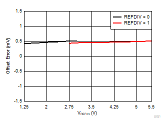
Figure 21. Offset Error vs Reference Voltage
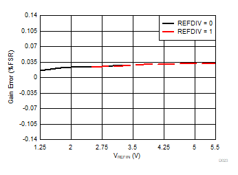
DAC80508 DAC70508 DAC60508 D023.gif
Gain = 1
Figure 23. Gain Error vs Reference Voltage
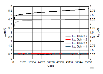
DAC80508 DAC70508 DAC60508 D025.gif
Gain = 1. External Reference = 2.5 V
Figure 25. Supply Current with External Reference vs
Digital Input Code
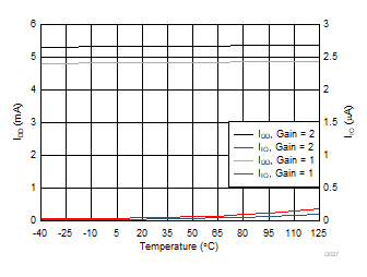
DAC80508 DAC70508 DAC60508 D027.gif
Gain = 1. External Reference = 2.5 V
Figure 27. Supply Current with External Reference vs
Temperature
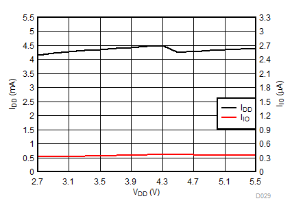
DAC80508 DAC70508 DAC60508 D029.gif
Gain = 1. External Reference = 2.5 V
Figure 29. Supply Current with External Reference vs
Supply Voltage
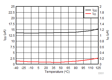
DAC80508 DAC70508 DAC60508 D031.gif
Figure 31. Power Down Current vs Temperature
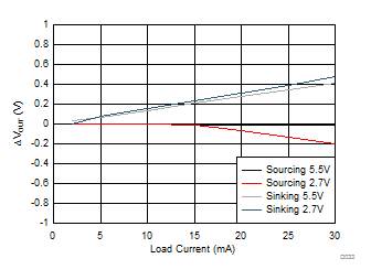
DAC80508 DAC70508 DAC60508 D033.gif
Figure 33. Headroom/Footroom vs Load Current
DAC80508 DAC70508 DAC60508 D035.gif
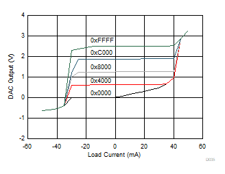
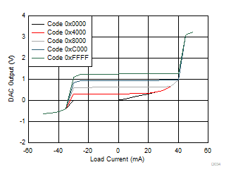
Figure 35. Source and Sink Capability with Gain = 1
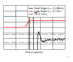
DAC80508 DAC70508 DAC60508 D037.gif
Gain = 1
Figure 37. Full-Scale Settling Time, Rising Edge
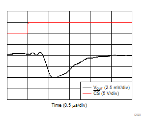
DAC80508 DAC70508 DAC60508 D039.gif
Gain = 1
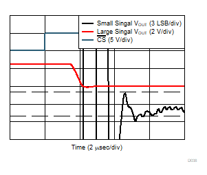
Figure 39. Glitch Impulse, Falling Edge, 1 LSB Step
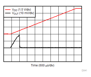
DAC80508 DAC70508 DAC60508 D041.gif
Gain = 1
Figure 41. Power-On, Reset to Zero Scale
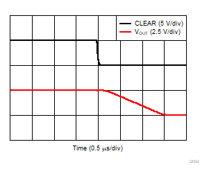
DAC80508 DAC70508 DAC60508 D059.gif
Gain = 1
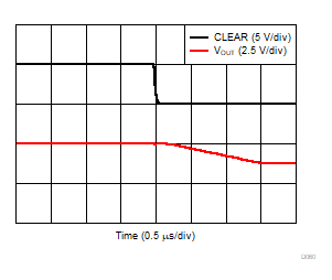
Figure 43. DACx0508C, Clear to Zero Scale
DAC80508 DAC70508 DAC60508 D043.gif
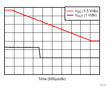
Gain = 1. DAC code at midscale
Figure 45. VDD Power-Down
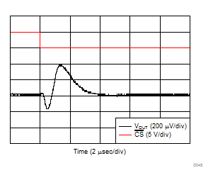
DAC80508 DAC70508 DAC60508 D045.gif
Gain = 1. Measured DAC at midscale. All other DACs switch from code 32 to full scale
Figure 47. Channel to Channel Crosstalk
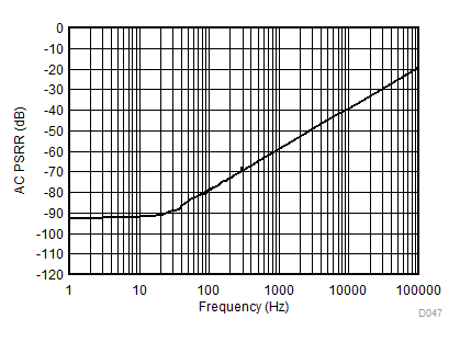
DAC80508 DAC70508 DAC60508 D047.gif
Gain = 1. VDD = 5 V + 200 mVPP (Sinusoid). DAC code at fullscale
Figure 49. DAC Output AC PSRR vs Frequency
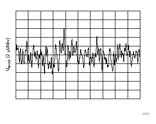
DAC80508 DAC70508 DAC60508 D049.gif
Gain = 1. External Reference = 2.5 V. DAC code at midscale
Figure 51. DAC Output Noise with External Reference
0.1 Hz to 10 Hz
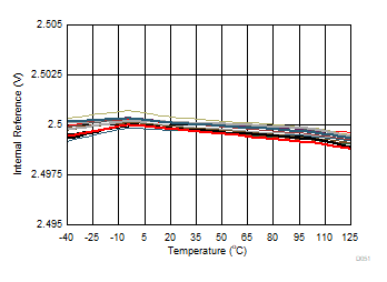
DAC80508 DAC70508 DAC60508 D051.gif
Figure 53. Internal Reference Voltage vs Temperature
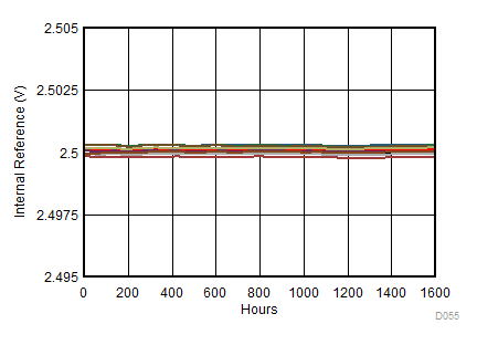
DAC80508 DAC70508 DAC60508 D055.gif
Figure 55. Internal Reference Voltage vs Time
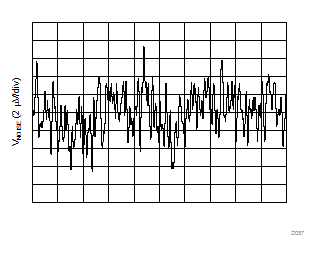
DAC80508 DAC70508 DAC60508 D057.gif
0.1 Hz to 10 Hz
Figure 57. Internal Reference Noise
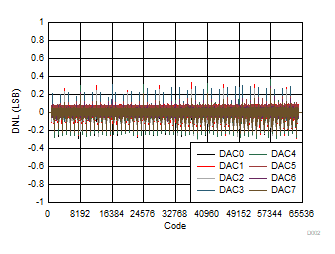
DAC80508 DAC70508 DAC60508 D002.gif
Figure 2. Differential Linearity Error vs Digital Input Code
DAC80508 DAC70508 DAC60508 D004.gif
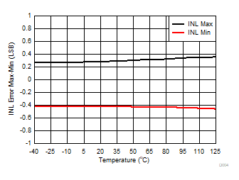
Figure 4. Integral Linearity Error vs Temperature
DAC80508 DAC70508 DAC60508 D006.gif
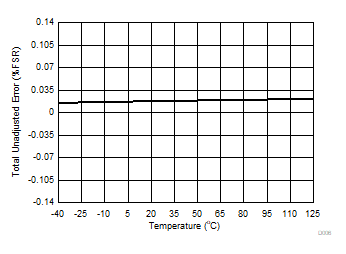
Figure 6. Total Unadjusted Error vs Temperature
DAC80508 DAC70508 DAC60508 D008.gif
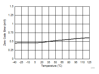
Figure 8. Zero Code Error vs Temperature
DAC80508 DAC70508 DAC60508 D010.gif
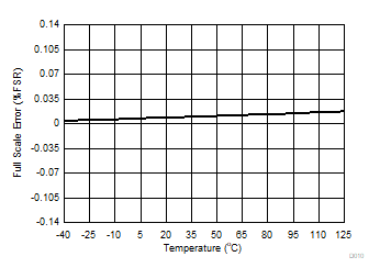
Figure 10. Full Scale Error vs Temperature
DAC80508 DAC70508 DAC60508 D012.gif
Gain = 1
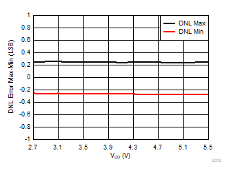
Figure 12. Differential Linearity Error vs Supply Voltage
DAC80508 DAC70508 DAC60508 D014.gif
Gain = 1
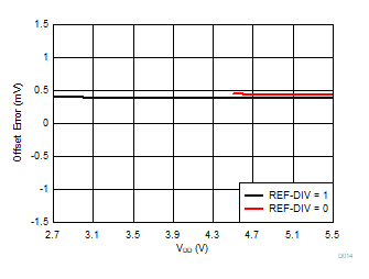
Figure 14. Offset Error vs Supply Voltage
DAC80508 DAC70508 DAC60508 D016.gif
Gain = 1
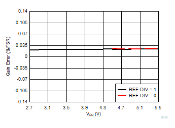
Figure 16. Gain Error vs Supply Voltage
DAC80508 DAC70508 DAC60508 D018.gif
Gain = 1
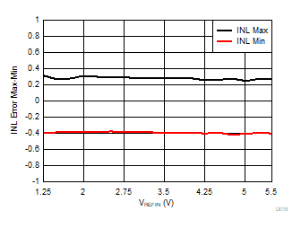
Figure 18. Integral Linearity Error vs Reference Voltage
DAC80508 DAC70508 DAC60508 D020.gif
Gain = 1
Figure 20. Total Unadjusted Error vs Reference Voltage
DAC80508 DAC70508 DAC60508 D022.gif
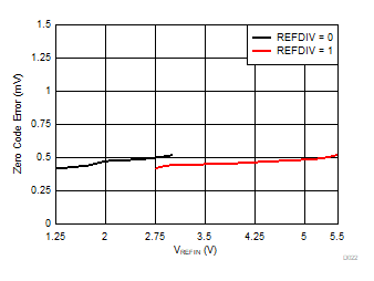
Gain = 1
Figure 22. Zero Code Error vs Reference Voltage
DAC80508 DAC70508 DAC60508 D024.gif
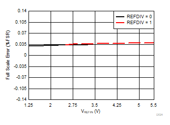
Gain = 1
Figure 24. Full Scale Error vs Reference Voltage
DAC80508 DAC70508 DAC60508 D026.gif
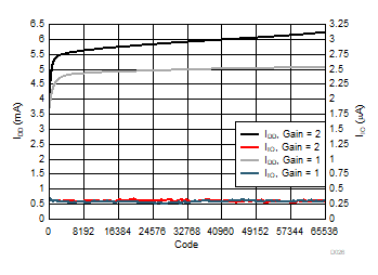
Gain = 1
Figure 26. Supply Current with Internal Reference vs
Digital Input Code
DAC80508 DAC70508 DAC60508 D028.gif
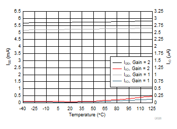
Gain = 1
Figure 28. Supply Current with Internal Reference vs
Temperature
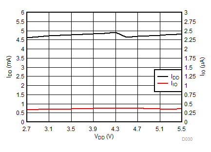
DAC80508 DAC70508 DAC60508 D030.gif
Gain = 1
Figure 30. Supply Current with Internal Reference vs
Supply Voltage
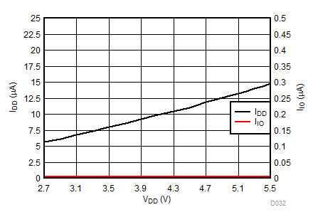
DAC80508 DAC70508 DAC60508 D032.gif
Figure 32. Power Down Current vs Supply Voltage
DAC80508 DAC70508 DAC60508 D034.gif
Figure 34. Source and Sink Capability with Gain = ½
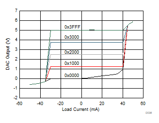
DAC80508 DAC70508 DAC60508 D036.gif
Figure 36. Source and Sink Capability with Gain = 2
DAC80508 DAC70508 DAC60508 D038.gif
Gain = 1
Figure 38. Full-Scale Settling Time, Falling Edge
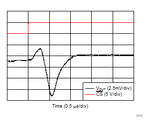
DAC80508 DAC70508 DAC60508 D040.gif
Gain = 1
Figure 40. Glitch Impulse, Rising Edge, 1 LSB Step
DAC80508 DAC70508 DAC60508 D042.gif
Gain = 1
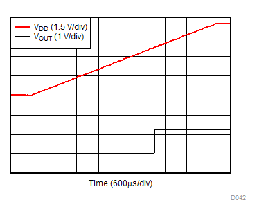
Figure 42. Power-On, Reset to Midscale
DAC80508 DAC70508 DAC60508 D060.gif
Gain = 1
Figure 44. DACx0508C, Clear to Midscale
DAC80508 DAC70508 DAC60508 D060_SLASEL1.gif
Gain = 1. DAC code at midscale
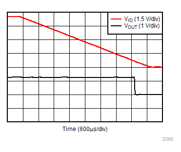
Figure 46. VIO Power-Down
DAC80508 DAC70508 DAC60508 D046.gif
Gain = 1. DAC code at midscale
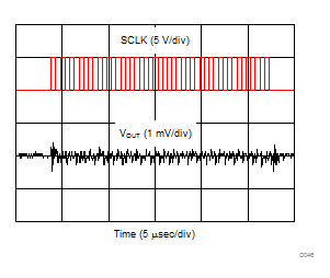
Figure 48. Clock Feedthrough with SCLK = 1 MHz
DAC80508 DAC70508 DAC60508 D048.gif
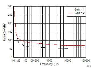
External Reference = 2.5 V. DAC code at midscale
Figure 50. DAC Output Noise Density vs Frequency
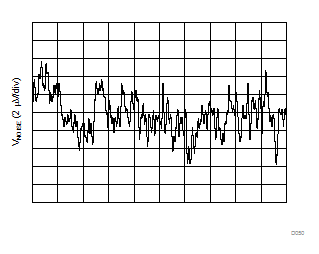
DAC80508 DAC70508 DAC60508 D050.gif
Gain = 1. DAC code at midscale
Figure 52. DAC Output Noise with Internal Reference
0.1 Hz to 10 Hz
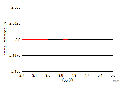
DAC80508 DAC70508 DAC60508 D052.gif
Figure 54. Internal Reference Voltage vs Supply Voltage
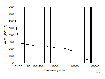
DAC80508 DAC70508 DAC60508 D056_SLASEL1.gif
Figure 56. Internal Reference Noise Density vs Frequency
DAC80508 DAC70508 DAC60508 D058.gif
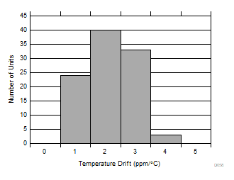
Figure 58. Internal Reference Temperature Drift Histogram