ZHCSH64D June 2017 – August 2018 DAC60508 , DAC70508 , DAC80508
PRODUCTION DATA.
- 1 特性
- 2 应用
- 3 说明
- 4 修订历史记录
- 5 Device Comparison Table
- 6 Pin Configuration and Functions
- 7 Specifications
-
8 Detailed Description
- 8.1 Overview
- 8.2 Functional Block Diagram
- 8.3 Feature Description
- 8.4 Device Functional Modes
- 8.5 Programming
- 8.6
Register Map
- 8.6.1 NOP Register (address = 0x00) [reset = 0x0000]
- 8.6.2 DEVICE ID Register (address = 0x01) [reset = 0x---]
- 8.6.3 SYNC Register (address = 0x2) [reset = 0xFF00]
- 8.6.4 CONFIG Register (address = 0x3) [reset = 0x0000]
- 8.6.5 GAIN Register (address = 0x04) [reset = 0x---]
- 8.6.6 TRIGGER Register (address = 0x05) [reset = 0x0000]
- 8.6.7 BRDCAST Register (address = 0x6) [reset = 0x0000]
- 8.6.8 STATUS Register (address = 0x7) [reset = 0x0000]
- 8.6.9 DACx Register (address = 0x8 to 0xF) [reset = 0x0000 or 0x8000]
- 9 Application and Implementation
- 10Power Supply Recommendations
- 11Layout
- 12器件和文档支持
- 13机械、封装和可订购信息
封装选项
机械数据 (封装 | 引脚)
散热焊盘机械数据 (封装 | 引脚)
- RTE|16
订购信息
8.3.3.1 Power-on-Reset (POR)
The DACx0508 includes a power-on reset function that controls the output voltage at power up. After the VDD and VIO supplies have been established a POR event is issued. The POR causes all registers to initialize to their default values and communication with the device is valid only after a 250 µs power-on-reset delay. The default value for all DACs in the DACx0508Z devices is zero-code and midscale-code for the DACx0508M ones. Each DAC channel remains at the power-up voltage until a valid command is written to it.
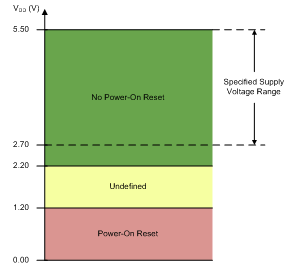
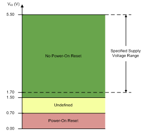
The POR circuit requires specific supply levels to discharge the internal capacitors and to reset the device on power up, as indicated in Figure 62 and Figure 63. In order to ensure a POR event, VDD or VIO must be below their corresponding low thresholds for at least 100 µs. If VDD and VIO remain above their specified high threshold a POR event will not occur. When the supplies drop below their high threshold but remain over the lower one (shown as the undefined region), the device may or may not reset under all specified temperature and power-supply conditions.
 Figure 62. Threshold Levels for VDD POR Circuit
  Figure 63. Threshold Levels for VIO POR Circuit