ZHCSH64D June 2017 – August 2018 DAC60508 , DAC70508 , DAC80508
PRODUCTION DATA.
- 1 特性
- 2 应用
- 3 说明
- 4 修订历史记录
- 5 Device Comparison Table
- 6 Pin Configuration and Functions
- 7 Specifications
-
8 Detailed Description
- 8.1 Overview
- 8.2 Functional Block Diagram
- 8.3 Feature Description
- 8.4 Device Functional Modes
- 8.5 Programming
- 8.6
Register Map
- 8.6.1 NOP Register (address = 0x00) [reset = 0x0000]
- 8.6.2 DEVICE ID Register (address = 0x01) [reset = 0x---]
- 8.6.3 SYNC Register (address = 0x2) [reset = 0xFF00]
- 8.6.4 CONFIG Register (address = 0x3) [reset = 0x0000]
- 8.6.5 GAIN Register (address = 0x04) [reset = 0x---]
- 8.6.6 TRIGGER Register (address = 0x05) [reset = 0x0000]
- 8.6.7 BRDCAST Register (address = 0x6) [reset = 0x0000]
- 8.6.8 STATUS Register (address = 0x7) [reset = 0x0000]
- 8.6.9 DACx Register (address = 0x8 to 0xF) [reset = 0x0000 or 0x8000]
- 9 Application and Implementation
- 10Power Supply Recommendations
- 11Layout
- 12器件和文档支持
- 13机械、封装和可订购信息
封装选项
机械数据 (封装 | 引脚)
散热焊盘机械数据 (封装 | 引脚)
- RTE|16
订购信息
9.1.2 Programmable Current Source Circuit
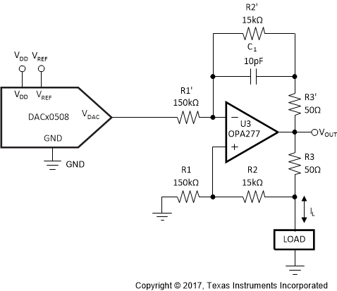
The DACx0508 can be integrated into the circuit in Figure 77 to implement an improved Howland current pump for precise voltage to current conversions. Bidirectional current flow and high voltage compliance are two features of the circuit. With a matched resistor network, the load current of the circuit is shown by Equation 2.

The value of R3 in Equation 2 can be reduced to increase the output current drive of U3. U3 can drive ±20 mV in both directions with voltage compliance limited up to 15 V by the U3 voltage supply. Elimination of the circuit compensation capacitor C1 in the circuit is not suggested as a result of the change in the output impedance ZO, according to Equation 3.

As shown in Equation 3, with matched resistors, ZO is infinite and the circuit is optimum for use as a current source. However, if unmatched resistors are used, ZO is positive or negative with negative output impedance being a potential cause of oscillation. Therefore, by incorporating C1 into the circuit, possible oscillation problems are eliminated. The value of C1 can be determined for critical applications; for most applications, however, a value of several pF is suggested.
 Figure 77. Programmable Bidirectional Current Source Circuit