ZHCS226B June   2011  – March 2015 DAC7551-Q1

PRODUCTION DATA.  

  1. 特性
  2. 应用
  3. 说明
  4. 修订历史记录
  5. Pin Configuration and Functions
  6. Specifications
    1. 6.1 Absolute Maximum Ratings
    2. 6.2 ESD Ratings
    3. 6.3 Recommended Operating Conditions
    4. 6.4 Thermal Information
    5. 6.5 Electrical Characteristics
    6. 6.6 Timing Requirements
    7. 6.7 Typical Characteristics
  7. Detailed Description
    1. 7.1 Overview
    2. 7.2 Functional Block Diagram
    3. 7.3 Feature Description
      1. 7.3.1 Digital-to-Analog Converter
      2. 7.3.2 Resistor String
      3. 7.3.3 Output Buffer Amplifiers
        1. 7.3.3.1 DAC External Reference Input
        2. 7.3.3.2 Amplifier Sense Input
        3. 7.3.3.3 Power-On Reset
        4. 7.3.3.4 Power Down
        5. 7.3.3.5 Asynchronous Clear
        6. 7.3.3.6 IOVDD and Level Shifters
      4. 7.3.4 Integral and Differential Linearity
      5. 7.3.5 Glitch Energy
    4. 7.4 Device Functional Modes
    5. 7.5 Programming
      1. 7.5.1 Serial Interface
        1. 7.5.1.1 16-Bit Word and Input Shift Register
        2. 7.5.1.2 Daisy-Chain Operation
  8. Application and Implementation
    1. 8.1 Application Information
      1. 8.1.1 Waveform Generation
      2. 8.1.2 Generating ±5-V, ±10-V, and ±12-V Outputs For Precision Industrial Control
        1. 8.1.2.1 Loop Accuracy
        2. 8.1.2.2 Loop Speed
    2. 8.2 Typical Application
      1. 8.2.1 Generating Industrial Voltage Ranges
        1. 8.2.1.1 Design Requirements
        2. 8.2.1.2 Detailed Design Procedure
        3. 8.2.1.3 Application Curves
  9. Power Supply Recommendations
  10. 10Layout
    1. 10.1 Layout Guidelines
    2. 10.2 Layout Example
  11. 11器件和文档支持
    1. 11.1 文档支持
      1. 11.1.1 相关文档
    2. 11.2 商标
    3. 11.3 静电放电警告
    4. 11.4 术语表
  12. 12机械封装和可订购信息

封装选项

机械数据 (封装 | 引脚)
散热焊盘机械数据 (封装 | 引脚)
订购信息

10 Layout

10.1 Layout Guidelines

A precision analog component requires careful layout, adequate bypassing, and clean, well-regulated power supplies. The DAC7551-Q1 device offers single-supply operation, and is often used in close proximity with digital logic, microcontrollers, microprocessors, digital signal processors, or a combination. The more digital logic present in the design and the higher the switching speed, the more difficult it is to prevent digital noise from appearing at the output. As a result of the single ground pin of the DAC7551-Q1 device, all return currents (including digital and analog return currents for the DAC) must flow through a single point. Ideally, the GND should be connected directly to an analog ground plane. This plane should be separate from the ground connection for the digital components until these components were connected at the power-entry point of the system.

10.2 Layout Example
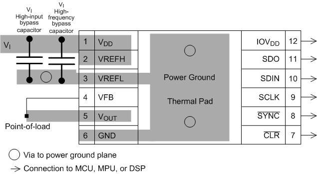
DAC7551-Q1 layout_slas767.gifFigure 32. DAC7551-Q1 Layout Example