ZHCS226B June 2011 – March 2015 DAC7551-Q1
PRODUCTION DATA.
- 1 特性
- 2 应用
- 3 说明
- 4 修订历史记录
- 5 Pin Configuration and Functions
- 6 Specifications
- 7 Detailed Description
- 8 Application and Implementation
- 9 Power Supply Recommendations
- 10Layout
- 11器件和文档支持
- 12机械封装和可订购信息
7 Detailed Description
7.1 Overview
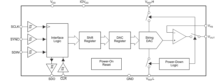
The DAC7551-Q1 device is a 12-bit resistor-string digital-to-analog converter (DAC). Unbuffered external reference inputs allow for a positive voltage reference as low as 0.25 V and as high as VDD. An amplifier-feedback input is available for better DC accuracy at the load point. The device is controlled over a 16-bit word three-wire serial peripheral interface (SPI) up to 50 MHz with an option to daisy-chain multiple devices. An asynchronous clear function along with power-down features allows for software controlled resets and low-power consumption. A separate logic-supply input means the device can be used with different logic families across a wide range of supply voltages.
7.2 Functional Block Diagram

7.3 Feature Description
7.3.1 Digital-to-Analog Converter
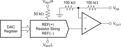
The architecture of the DAC7551-Q1 device consists of a string DAC followed by an output buffer amplifier. Figure 26 shows a generalized block diagram of the DAC architecture.
 Figure 26. Typical DAC Architecture
The input coding to the DAC7551-Q1 device is unsigned binary, which gives the ideal output voltage as show in Equation 1.
where
- D is the decimal equivalent of the binary code that is loaded to the DAC register, which ranges from 0 to 4095.
7.3.2 Resistor String
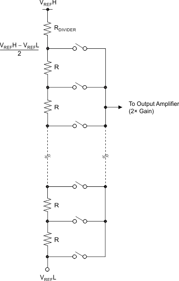
Figure 27 shows the resistor string section. This section is simply a string of resistors, each of value R. The digital code loaded to the DAC register determines at which node on the string the voltage is tapped off to be fed into the output amplifier. The voltage is tapped off by closing one of the switches connecting the string to the amplifier. The output of the DAC is specified monotonic because it is a string of resistors.
 Figure 27. Typical Resistor String
7.3.3 Output Buffer Amplifiers
The output buffer amplifier is capable of generating rail-to-rail voltages on the output, providing an output range of 0 V to VDD. The amplifier is capable of driving a load of 2 kΩ in parallel with up to 1000 pF to ground. Figure 8, Figure 9, and Figure 10 show the sink and source capabilities of the output amplifier. The slew rate is 1.8 V/μs with a half-scale settling time of 3 μs with the output unloaded.
7.3.3.1 DAC External Reference Input
The DAC7551-Q1 device contains VREFH and VREFL reference inputs which are unbuffered. The VREFH reference voltage can be as low as 0.25 V, and as high as VDD because there is no restriction of headroom and footroom from any reference amplifier.
Using a buffered reference in the external circuit is recommended (for example, the REF3140 device). The input impedance is typically 100 kΩ.
7.3.3.2 Amplifier Sense Input
The DAC7551-Q1 device contains an amplifier-feedback input pin, VFB. For voltage output operation, VFB must be externally connected to VOUT. For better DC accuracy, this connection should be made at load points. The VFB pin is also useful for a variety of applications, including digitally-controlled current sources. The feedback input pin is internally connected to the DAC amplifier negative input terminal through a 100-kΩ resistor. The amplifier negative input terminal internally connects to ground through another 100-kΩ resistor (see Figure 26). These connections form a gain-of-two, noninverting, amplifier configuration. Overall gain remains 1 because the resistor string has a divide-by-two configuration. The resistance seen at the VFB pin is approximately 200 kΩ to ground.
7.3.3.3 Power-On Reset
On power up, all registers are cleared and the DAC channel is updated with zero-scale voltage. The DAC output remains in this state until valid data are written. This setup is particularly useful in applications where knowing the state of the DAC output while the device is powering up is important. To not turn on ESD protection devices, VDD and IOVDD should be applied before any other pin (such as VREFH) is brought high. The power-up sequence of VDD and IOVDD is irrelevant. Therefore, IOVDD can be brought up before VDD, or the other way around.
7.3.3.4 Power Down
The DAC7551-Q1 device has a flexible power-down capability. During a power-down condition, the user has flexibility to select the output impedance of the DAC. During power-down operation, the DAC can have either 1kΩ, 100kΩ, or Hi-Z output impedance to ground.
7.3.3.5 Asynchronous Clear
The DAC7551-Q1 output is asynchronously set to zero-scale voltage immediately after the CLR pin is brought low. The CLR signal resets all internal registers and therefore functions similar to the power-on reset. The DAC7551-Q1 device updates at the first rising edge of the SYNC signal that occurs after the CLR pin is brought back to high.
7.3.3.6 IOVDD and Level Shifters
The DAC7551-Q1 device can be used with different logic families that require a wide range of supply voltages. To enable this useful feature, the IOVDD pin must be connected to the logic supply voltage of the system. All DAC7551-Q1 digital input and output pins are equipped with level-shifter circuits. Level shifters at the input pins ensure that external logic-high voltages are translated to the internal logic-high voltage, with no additional power dissipation. Similarly, the level shifter for the SDO pin translates the internal logic-high voltage (VDD) to the external logic-high level (IOVDD). For single-supply operation, the IOVDD pin can be tied to the VDD pin.
7.3.4 Integral and Differential Linearity
The DAC7551-Q1 device uses precision thin-film resistors providing exceptional linearity and monotonicity. Integral linearity error is typically within ±0.35 LSBs, and differential linearity error is typically within ±0.08 LSBs.
7.3.5 Glitch Energy
The DAC7551-Q1 device uses a proprietary architecture that minimizes glitch energy. The code-to-code glitches are so low that they are usually buried within the wide-band noise and cannot be easily detected. The
DAC7551-Q1 glitch is typically well under 0.1 nV-s. Such low glitch energy provides more than a ten-time improvement over industry alternatives.
7.4 Device Functional Modes
The DAC7551-Q1 device uses four modes of operation. These modes are accessed by setting bit PD0 (DB13) and PD1 (DB14) in the control register. Table 1 shows how to control the operating mode with data bits PD0 (DB13) and PD1 (DB14). The DAC7551-Q1 device treats the power-down condition as data; all the operation modes are still valid for power down. Broadcasting a power-down condition to all the DAC7551-Q1 devices in a system is possible. Powering down a channel and updating data on other channels is also possible. Furthermore, writing to the DAC register or buffer of the DAC channel that is powered down is also possible. When the DAC is the powered on, the DAC contains this new value.
When both the PD0 and PD1 bits are set to 0, the device works normally with the typical consumption of 100 µA at 2.7 V. For the three power-down modes, the supply current falls to 0.05 µA at 2.7 V. As listed in Table 1, three different power-down options are available. The VOUT pin can be connected internally to GND through a 1-kΩ resistor or a 100-kΩ resistor or can be open circuited (High-Z). In other words, DB14 and DB13 = 11 represent a power-down condition with High-Z output impedance for a selected channel. DB14 and DB13 = 01 and 10 represent a power-down condition with a 1-kΩ and 100-kΩ output impedance respectively.
7.5 Programming
7.5.1 Serial Interface
The DAC7551-Q1 device is controlled over a versatile 3-wire serial interface, which operates at clock rates up to 50 MHz and is compatible with SPI, QSPI, Microwire, and DSP interface standards.
Table 1. Serial Interface Programming
| CONTROL | DATA BITS | FUNCTION | |||
|---|---|---|---|---|---|
| DB15 | DB14 | DB13 (PD1) |
DB12 (PD0) |
DB11–DB0 | |
| X | X | 0 | 0 | data | Normal mode |
| X | X | 0 | 1 | X | Powerdown 1kΩ |
| X | X | 1 | 0 | X | Powerdown 100kΩ |
| X | X | 1 | 1 | X | Powerdown Hi-Z |
7.5.1.1 16-Bit Word and Input Shift Register
The input shift register is 16 bits wide. DAC data are loaded into the device as a 16-bit word under the control of a serial clock input, SCLK, as shown in Figure 1. The 16-bit word, listed in Table 1, consists of four control bits followed by 12 bits of DAC data. The data format is straight binary with all 0s corresponding to 0-V output and all 1s corresponding to full-scale output (VREF – 1 LSB). Data are loaded MSB first (bit 15) where the first two bits (DB15 and DB14) are don't care bits. Bit 13 and bit 12 (DB13 and DB12) determine either normal mode operation or power-down mode (see Table 1).
The SYNC input is a level-triggered input that acts as a frame synchronization signal and chip enable. Data can only be transferred into the device while the SYNC pin is low. To begin the serial data transfer, the SYNC pin should be taken low, observing the minimum SYNC-to-SCLK falling edge setup time, t4. After the SYNC pin goes low, serial data is shifted into the device input shift register on the falling edges of SCLK for 16 clock pulses.
The SPI is enabled after the SYNC pin becomes low and the data are continuously shifted into the shift register at each falling edge of the SCLK input. When the SYNC pin is brought high, the last 16 bits stored in the shift register are latched into the DAC register, and the DAC updates.
7.5.1.2 Daisy-Chain Operation
Daisy-chain operation is used for updating serially-connected devices on the rising edge of the SYNC in.
As long as the SYNC pin is high, the SDO pin is in a high-impedance state. When the SYNC pin is brought low the output of the internal shift register is tied to the SDO pin. As long as the SYNC pin is low, the SDO pin duplicates the SDIN signal with a 16-cycle delay. To support multiple devices in a daisy chain, the SCLK and SYNC signals are shared across all devices, and the SDO pin of one DAC7551-Q1 device should be tied to the SDIN pin of the next DAC7551-Q1 device. For n devices in such a daisy chain, 16n SCLK cycles are required to shift the entire input data stream. After 16n SCLK falling edges are received, following a falling SYNC signal, the data stream becomes complete and the SYNC pin can be brought high to update n devices simultaneously. SDO operation is specified at a maximum SCLK speed of 10 MHz.
In daisy-chain mode, the use of a weak pulldown resistor on the SDO output pin, which provides the SDIN data for the next device in the chain, is recommended. For standalone operation, the maximum clock speed is
50 MHz. For daisy-chain operation, the maximum clock speed is 10 MHz.