ZHCSC70D December   2013  – December 2021 DAC7750 , DAC8750

PRODUCTION DATA  

  1. 特性
  2. 应用
  3. 说明
  4. Revision History
  5. Device Comparison Table
  6. Pin Configuration and Functions
  7. Specifications
    1. 7.1  Absolute Maximum Ratings
    2. 7.2  ESD Ratings
    3. 7.3  Recommended Operating Conditions
    4. 7.4  Thermal Information
    5. 7.5  Electrical Characteristics
    6. 7.6  Electrical Characteristics: AC
    7. 7.7  Timing Requirements: Write Mode
    8. 7.8  Timing Requirements: Readback Mode
    9. 7.9  Timing Diagrams
    10. 7.10 Typical Characteristics
  8. Detailed Description
    1. 8.1 Overview
    2. 8.2 Functional Block Diagram
    3. 8.3 Feature Description
      1. 8.3.1  DAC Architecture
      2. 8.3.2  Current Output Stage
      3. 8.3.3  Internal Reference
      4. 8.3.4  Digital Power Supply
      5. 8.3.5  DAC Clear
      6. 8.3.6  Power-On Reset
      7. 8.3.7  Alarm Detection
      8. 8.3.8  Watchdog Timer
      9. 8.3.9  Frame Error Checking
      10. 8.3.10 User Calibration
      11. 8.3.11 Programmable Slew Rate
    4. 8.4 Device Functional Modes
      1. 8.4.1 Setting Current-Output Ranges
      2. 8.4.2 Current-Setting Resistor
      3. 8.4.3 BOOST Configuration for IOUT
      4. 8.4.4 Filtering The Current Output
      5. 8.4.5 Output Current Monitoring
      6. 8.4.6 HART Interface
        1. 8.4.6.1 Implementing HART in 4-mA to 20-mA Mode
        2. 8.4.6.2 Implementing HART in All Current Output Modes
    5. 8.5 Programming
      1. 8.5.1 Serial Peripheral Interface (SPI)
        1. 8.5.1.1 SPI Shift Register
        2. 8.5.1.2 Write Operation
        3. 8.5.1.3 Read Operation
        4. 8.5.1.4 Stand-Alone Operation
        5. 8.5.1.5 Multiple Devices on the Bus
    6. 8.6 Register Maps
      1. 8.6.1 DACx750 Register Descriptions
        1. 8.6.1.1 Control Register
        2. 8.6.1.2 Configuration Register
        3. 8.6.1.3 DAC Registers
        4. 8.6.1.4 Reset Register
        5. 8.6.1.5 Status Register
  9. Application and Implementation
    1. 9.1 Application Information
      1. 9.1.1 HART Implementation
        1. 9.1.1.1 Using the CAP2 Pin
        2. 9.1.1.2 Using the ISET-R Pin
    2. 9.2 Typical Application
      1. 9.2.1 Design Requirements
      2. 9.2.2 Detailed Design Procedure
      3. 9.2.3 Application Curve
  10. 10Power Supply Recommendations
  11. 11Layout
    1. 11.1 Layout Guidelines
      1. 11.1.1 Thermal Considerations
    2. 11.2 Layout Example
  12. 12Device and Documentation Support
    1. 12.1 Documentation Support
      1. 12.1.1 Related Documentation
    2. 12.2 接收文档更新通知
    3. 12.3 支持资源
    4. 12.4 Trademarks
    5. 12.5 Electrostatic Discharge Caution
    6. 12.6 术语表
  13. 13Mechanical, Packaging, and Orderable Information

封装选项

机械数据 (封装 | 引脚)
散热焊盘机械数据 (封装 | 引脚)
订购信息

Application Curve

The current output circuit was measured in 0-mA to 24-mA mode using an 8.5 digit digital multimeter to measure the output while driving a 300-Ω load at 25°C. The measured results are illustrated in Figure 9-5. The current output remains within the data sheet specified performance.

The design was also exposed to IEC61000-4 electrostatic discharge, electrically fast transient, conducted immunity, and radiated immunity tests on both the current and voltage outputs. During each of these tests a 6.5 digit digital multimeter, set in fast 5.5 digit acquisition mode, was used to monitor the output. Complete data sets for the voltage and current outputs during these tests are available in the Single-Channel Industrial Voltage and Current Output Driver, Isolated, EMC/EMI Tested Reference Design.
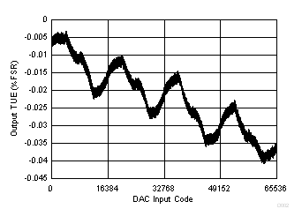
GUID-970548AD-9344-467D-9FAC-7437C30936B8-low.gif Figure 9-5 Current Output TUE vs Code