ZHCSC70D December   2013  – December 2021 DAC7750 , DAC8750

PRODUCTION DATA  

  1. 特性
  2. 应用
  3. 说明
  4. Revision History
  5. Device Comparison Table
  6. Pin Configuration and Functions
  7. Specifications
    1. 7.1  Absolute Maximum Ratings
    2. 7.2  ESD Ratings
    3. 7.3  Recommended Operating Conditions
    4. 7.4  Thermal Information
    5. 7.5  Electrical Characteristics
    6. 7.6  Electrical Characteristics: AC
    7. 7.7  Timing Requirements: Write Mode
    8. 7.8  Timing Requirements: Readback Mode
    9. 7.9  Timing Diagrams
    10. 7.10 Typical Characteristics
  8. Detailed Description
    1. 8.1 Overview
    2. 8.2 Functional Block Diagram
    3. 8.3 Feature Description
      1. 8.3.1  DAC Architecture
      2. 8.3.2  Current Output Stage
      3. 8.3.3  Internal Reference
      4. 8.3.4  Digital Power Supply
      5. 8.3.5  DAC Clear
      6. 8.3.6  Power-On Reset
      7. 8.3.7  Alarm Detection
      8. 8.3.8  Watchdog Timer
      9. 8.3.9  Frame Error Checking
      10. 8.3.10 User Calibration
      11. 8.3.11 Programmable Slew Rate
    4. 8.4 Device Functional Modes
      1. 8.4.1 Setting Current-Output Ranges
      2. 8.4.2 Current-Setting Resistor
      3. 8.4.3 BOOST Configuration for IOUT
      4. 8.4.4 Filtering The Current Output
      5. 8.4.5 Output Current Monitoring
      6. 8.4.6 HART Interface
        1. 8.4.6.1 Implementing HART in 4-mA to 20-mA Mode
        2. 8.4.6.2 Implementing HART in All Current Output Modes
    5. 8.5 Programming
      1. 8.5.1 Serial Peripheral Interface (SPI)
        1. 8.5.1.1 SPI Shift Register
        2. 8.5.1.2 Write Operation
        3. 8.5.1.3 Read Operation
        4. 8.5.1.4 Stand-Alone Operation
        5. 8.5.1.5 Multiple Devices on the Bus
    6. 8.6 Register Maps
      1. 8.6.1 DACx750 Register Descriptions
        1. 8.6.1.1 Control Register
        2. 8.6.1.2 Configuration Register
        3. 8.6.1.3 DAC Registers
        4. 8.6.1.4 Reset Register
        5. 8.6.1.5 Status Register
  9. Application and Implementation
    1. 9.1 Application Information
      1. 9.1.1 HART Implementation
        1. 9.1.1.1 Using the CAP2 Pin
        2. 9.1.1.2 Using the ISET-R Pin
    2. 9.2 Typical Application
      1. 9.2.1 Design Requirements
      2. 9.2.2 Detailed Design Procedure
      3. 9.2.3 Application Curve
  10. 10Power Supply Recommendations
  11. 11Layout
    1. 11.1 Layout Guidelines
      1. 11.1.1 Thermal Considerations
    2. 11.2 Layout Example
  12. 12Device and Documentation Support
    1. 12.1 Documentation Support
      1. 12.1.1 Related Documentation
    2. 12.2 接收文档更新通知
    3. 12.3 支持资源
    4. 12.4 Trademarks
    5. 12.5 Electrostatic Discharge Caution
    6. 12.6 术语表
  13. 13Mechanical, Packaging, and Orderable Information

封装选项

机械数据 (封装 | 引脚)
散热焊盘机械数据 (封装 | 引脚)
订购信息

Using the ISET-R Pin

The second method to implement HART is to couple the HART signal through the ISET-R pin when IOUT is operated using an external RSET resistor. The FSK signal from the modem is ac-coupled into the pin through a series combination of Rin and Cin as shown in Figure 9-2.
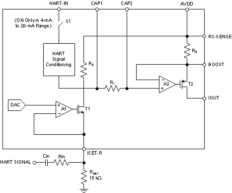
GUID-7ED8CF4F-D744-4AD0-A632-7076E846ED84-low.gifFigure 9-2 Implementing HART with the ISET-R pin

The magnitude of the ac-current output is calculated with Equation 6.

Equation 6. (VHART × k) / Rin

where

  • VHART is the amplitude of the HART FSK signal from the modem
  • k is a constant that represents the gain transfer function from the ISET-R pin to the IOUT pin and depends on the selected current output range as follows:
    • k = 60 for the 4-mA to 20-mA range
    • k = 75 for the 0-mA to 20-mA range
    • k = 90 for the 0-mA to 24-mA range

The series input resistor and capacitor form a high-pass filter at the ISET-R pin. Select Cin to make sure that all signals in the HART extended-frequency band pass through unattenuated.