ZHCSBX4D June 2013 – December 2021 DAC7760 , DAC8760
PRODUCTION DATA
- 1 特性
- 2 应用
- 3 说明
- 4 Revision History
- 5 Device Comparison Table
- 6 Pin Configuration and Functions
- 7 Specifications
- 8 Detailed Description
- 9 Application and Implementation
- 10Power Supply Recommendations
- 11Layout
- 12Device and Documentation Support
- 13Mechanical, Packaging, and Orderable Information
封装选项
机械数据 (封装 | 引脚)
散热焊盘机械数据 (封装 | 引脚)
订购信息
8.3.3 Current Output Stage
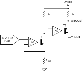
The current output stage consists of a
preconditioner and a current source as
conceptualized in Figure 8-3. This stage provides a current output according
to the DAC code. The output range can be
programmed as 0 mA to
20 mA, 0 mA to 24 mA, or 4 mA to 20 mA. An
external boost transistor can be used to reduce
the power dissipation of the device. The maximum
compliance voltage on pin IOUT equals (AVDD – 2
V). In single power-supply mode, the maximum AVDD
is 36 V, and the maximum compliance voltage is 34
V. After power on, the IOUT pin is in a Hi-Z
state.
 Figure 8-3 Current Output
Resistor RSET (used to convert the DAC voltage to current) determines the stability of the output current over temperature. If desired, an external, low-drift, precision 15-kΩ resistor can be connected to the ISET-R pin and used instead of the internal RSET resistor.
For a 5-V reference, the output can be expressed as shown in Equation 3 through Equation 5.
For a 0-mA to 20-mA output range:

For a 0-mA to 24-mA output range:

For a 4-mA to 20-mA output range:

where
- CODE is the decimal equivalent of the code loaded to the DAC.
- N is the bits of resolution; 16 for DAC8760 and 12 for DAC7760.
The current-output range is normally set according to the value of the RANGE bits in the Control Register. When both the voltage and current outputs are enabled in dual-output mode, the range is set by the IOUT RANGE bits in the Configuration Register. See Section 8.4.1 for more details. For more details on controlling the current output when both the VOUT and IOUT pins are simultaneously enabled, see Section 9.1.1.