ZHCSHU4E April 2005 – March 2018 DAC7811
PRODUCTION DATA.
7.3 Feature Description
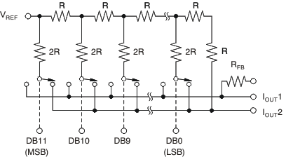
The DAC7811 is a single channel, current output, 12-bit digital-to-analog converter (DAC). The architecture, illustrated in Figure 25, is an R-2R ladder configuration with the three MSBs segmented. Each 2R leg of the ladder is either switched to IOUT1 or the IOUT2 terminal. The IOUT1 terminal of the DAC is held at a virtual GND potential by the use of an external I/V converter op amp. The R-2R ladder is connected to an external reference input VREF that determines the DAC full-scale current. The R-2R ladder presents a code independent load impedance to the external reference of 10kΩ ±20%. The external reference voltage can vary over a range of –15V to +15V, thus providing bipolar IOUT current operation. By using an external I/V converter and the DAC7811 RFB resistor, output voltage ranges of –VREF to VREF can be generated.
 Figure 25. Equivalent R-2R DAC Circuit
When using an external I/V converter and the DAC7811 RFB resistor, the DAC output voltage is given by Equation 1:

Each DAC code determines the 2R leg switch position to either GND or IOUT. Because the DAC output impedance as seen looking into the IOUT1 terminal changes versus code, the external I/V converter noise gain will also change. Because of this, the external I/V converter op amp must have a sufficiently low offset voltage such that the amplifier offset is not modulated by the DAC IOUT1 terminal impedance change. External op amps with large offset voltages can produce INL errors in the transfer function of the DAC7811 due to offset modulation versus DAC code.
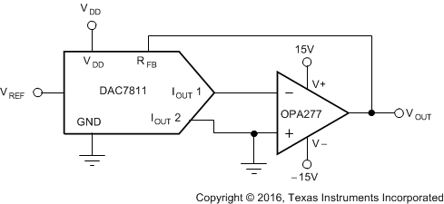
For best linearity performance of the DAC7811, a low offset voltage op amp (such as the OPA277) is recommended (see Figure 26). This circuit allows VREF swinging from –10 V to 10 V.
 Figure 26. Voltage Output Configuration