ZHCSKJ2A November 2019 – April 2020 DAC60502 , DAC70502 , DAC80502
PRODUCTION DATA.
- 1 特性
- 2 应用
- 3 说明
- 4 修订历史记录
- 5 Device Comparison Table
- 6 Pin Configuration and Functions
-
7 Specifications
- 7.1 Absolute Maximum Ratings
- 7.2 ESD Ratings
- 7.3 Recommended Operating Conditions
- 7.4 Thermal Information
- 7.5 Electrical Characteristics
- 7.6 Timing Requirements : SPI Mode
- 7.7 Timing Requirements : I2C Standard Mode
- 7.8 Timing Requirements : I2C Fast Mode
- 7.9 Timing Requirements : I2C Fast-Mode Plus
- 7.10 Typical Characteristics
-
8 Detailed Description
- 8.1 Overview
- 8.2 Functional Block Diagram
- 8.3 Feature Description
- 8.4 Device Functional Modes
- 8.5 Programming
- 8.6
Register Maps
- 8.6.1
Registers
- 8.6.1.1 NOOP Register (offset = 0h) [reset = 0000h]
- 8.6.1.2 DEVID Register (offset = 1h) [reset = 0214h for DAC80502, 1214h for DAC70502, 2214h for DAC60502]
- 8.6.1.3 SYNC Register (offset = 2h) [reset = 0300h]
- 8.6.1.4 CONFIG Register (offset = 3h) [reset = 0000h]
- 8.6.1.5 GAIN Register (offset = 4h) [reset = 0003h]
- 8.6.1.6 TRIGGER Register (offset = 5h) [reset = 0000h]
- 8.6.1.7 BRDCAST Register (offset = 6h) [reset = 0000h for RSTSEL = 0, or reset = 8000h for RSTSEL = 1]
- 8.6.1.8 STATUS Register (offset = 7h) [reset = 0000h]
- 8.6.1.9 DAC-n Register (offset = 8h–9h) [reset = 0000h for RSTSEL = 0, or reset = 8000h for RSTSEL = 1]
- 8.6.1
Registers
- 9 Application and Implementation
- 10Power Supply Recommendations
- 11Layout
- 12器件和文档支持
- 13机械、封装和可订购信息
7.9 Timing Requirements : I2C Fast-Mode Plus
all input signals are specified with tR = tF = 1 ns/V and timed from a voltage level of (VIL + VIH) / 2. 2.7 V ≤ VDD ≤ 5.5 V,VIH = 1.62 V, VIL = 0.45 V, VREFIO = 1.25 V to 5.5 V, and TA = – 40°C to +125°C (unless otherwise noted)
| MIN | NOM | MAX | UNIT | ||
|---|---|---|---|---|---|
| fSCLK | SCL frequency | 1 | MHz | ||
| tBUF | Bus free time between stop and start conditions | 0.5 | µs | ||
| tHDSTA | Hold time after repeated start | 0.26 | µs | ||
| tSUSTA | Repeated start setup time | 0.26 | µs | ||
| tSUSTO | Stop condition setup time | 0.26 | µs | ||
| tHDDAT | Data hold time | 0 | ns | ||
| tSUDAT | Data setup time | 50 | ns | ||
| tLOW | SCL clock low period | 500 | ns | ||
| tHIGH | SCL clock high period | 260 | ns | ||
| tR | Clock and data fall time | 120 | ns | ||
| tF | Clock and data rise time | 120 | ns | ||
| tUPDATE | Sequential DAC update wait time | 1 | µs | ||
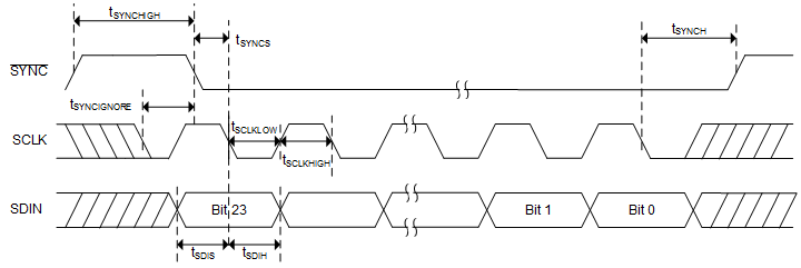
 Figure 1. SPI Mode Timing
  Figure 2. I2C Mode Timing