ZHCSKJ2A November 2019 – April 2020 DAC60502 , DAC70502 , DAC80502
PRODUCTION DATA.
- 1 特性
- 2 应用
- 3 说明
- 4 修订历史记录
- 5 Device Comparison Table
- 6 Pin Configuration and Functions
-
7 Specifications
- 7.1 Absolute Maximum Ratings
- 7.2 ESD Ratings
- 7.3 Recommended Operating Conditions
- 7.4 Thermal Information
- 7.5 Electrical Characteristics
- 7.6 Timing Requirements : SPI Mode
- 7.7 Timing Requirements : I2C Standard Mode
- 7.8 Timing Requirements : I2C Fast Mode
- 7.9 Timing Requirements : I2C Fast-Mode Plus
- 7.10 Typical Characteristics
-
8 Detailed Description
- 8.1 Overview
- 8.2 Functional Block Diagram
- 8.3 Feature Description
- 8.4 Device Functional Modes
- 8.5 Programming
- 8.6
Register Maps
- 8.6.1
Registers
- 8.6.1.1 NOOP Register (offset = 0h) [reset = 0000h]
- 8.6.1.2 DEVID Register (offset = 1h) [reset = 0214h for DAC80502, 1214h for DAC70502, 2214h for DAC60502]
- 8.6.1.3 SYNC Register (offset = 2h) [reset = 0300h]
- 8.6.1.4 CONFIG Register (offset = 3h) [reset = 0000h]
- 8.6.1.5 GAIN Register (offset = 4h) [reset = 0003h]
- 8.6.1.6 TRIGGER Register (offset = 5h) [reset = 0000h]
- 8.6.1.7 BRDCAST Register (offset = 6h) [reset = 0000h for RSTSEL = 0, or reset = 8000h for RSTSEL = 1]
- 8.6.1.8 STATUS Register (offset = 7h) [reset = 0000h]
- 8.6.1.9 DAC-n Register (offset = 8h–9h) [reset = 0000h for RSTSEL = 0, or reset = 8000h for RSTSEL = 1]
- 8.6.1
Registers
- 9 Application and Implementation
- 10Power Supply Recommendations
- 11Layout
- 12器件和文档支持
- 13机械、封装和可订购信息
8.5.1.2.1 F/S Mode Protocol
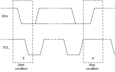
- The master initiates data transfer by generating a start condition. The start condition is when a high to-low transition occurs on the SDA line while SCL is high, as shown in Figure 60. All I2C-compatible devices recognize a start condition.
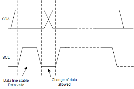
- The master then generates the SCL pulses, and transmits the 7-bit address and the read/write direction bit (R/W) on the SDA line. During all transmissions, the master makes sure that data are valid. A valid data condition requires the SDA line to be stable during the entire high period of the clock pulse, as shown in Figure 61. All devices recognize the address sent by the master and compare it to their internal fixed addresses. Only the slave device with a matching address generates an acknowledge by pulling the SDA line low during the entire high period of the 9th SCL cycle, as shown in Figure 59. Upon detecting this acknowledge, the master knows the communication link with a slave has been established.
- The master generates further SCL cycles to transmit (R/W bit 0) or receive (R/W bit 1) data to the slave. In either case, the receiver must acknowledge the data sent by the transmitter so that the acknowledge signal can be generated by the master or by the slave, depending on which one is the receiver. The 9-bit valid data sequences consists of eight data bits and one acknowledge-bit, and can continue for as long as necessary.
- To signal the end of the data transfer, the master generates a stop condition by pulling the SDA line from low-to-high while the SCL line is high (see Figure 60). This action releases the bus and stops the communication link with the addressed slave. All I2C-compatible devices recognize the stop condition. Upon receipt of a stop condition, the bus is released, and all slave devices then wait for a start condition followed by a matching address.
 Figure 60. Start and Stop Conditions
  Figure 61. Bit Transfer on the I2C Bus