SBAS246B December   2001  – November 2014 DAC8532

PRODUCTION DATA.  

  1. Features
  2. Applications
  3. Description
  4. Simplified Diagram
  5. Revision History
  6. Pin Configuration and Functions
  7. Specifications
    1. 7.1 Absolute Maximum Ratings
    2. 7.2 Handling Ratings
    3. 7.3 Recommended Operating Conditions
    4. 7.4 Thermal Information
    5. 7.5 Electrical Characteristics
    6. 7.6 Timing Requirements
    7. 7.7 Typical Characteristics
  8. Detailed Description
    1. 8.1 Overview
    2. 8.2 Functional Block Diagram
    3. 8.3 Feature Description
      1. 8.3.1 DAC Section
      2. 8.3.2 Resistor String
      3. 8.3.3 Output Amplifier
      4. 8.3.4 Serial Interface
      5. 8.3.5 Power-On Reset
    4. 8.4 Device Functional Modes
      1. 8.4.1 Input Shift Register
      2. 8.4.2 SYNC Interrupt
      3. 8.4.3 Power-Down Modes
    5. 8.5 Register Maps
      1. 8.5.1 Operation Examples
  9. Application and Implementation
    1. 9.1 Application Information
      1. 9.1.1 Current Consumption
      2. 9.1.2 Driving Resistive and Capacitive Loads
      3. 9.1.3 Crosstalk and AC Performance
      4. 9.1.4 Output Voltage Stability
      5. 9.1.5 Settling Time and Output Glitch Performance
      6. 9.1.6 Microprocessor Interfacing
        1. 9.1.6.1 DAC8532 to 8051 Interface
        2. 9.1.6.2 DAC8532 to Microwire Interface
        3. 9.1.6.3 DAC8532 to 68HC11 Interface
      7. 9.1.7 DAC8532 to TMS320 DSP Interface
      8. 9.1.8 Bipolar Operation Using the DAC8532
    2. 9.2 Typical Application
      1. 9.2.1 Using REF5050 as a Power Supply for DAC8532
        1. 9.2.1.1 Design Requirements
        2. 9.2.1.2 Detailed Design Procedure
        3. 9.2.1.3 Application Curves
  10. 10Power Supply Recommendations
  11. 11Layout
    1. 11.1 Layout Guidelines
    2. 11.2 Layout Example
  12. 12Device and Documentation Support
    1. 12.1 Trademarks
    2. 12.2 Electrostatic Discharge Caution
    3. 12.3 Glossary
  13. 13Mechanical, Packaging, and Orderable Information

封装选项

请参考 PDF 数据表获取器件具体的封装图。

机械数据 (封装 | 引脚)
  • DGK|8
散热焊盘机械数据 (封装 | 引脚)
订购信息

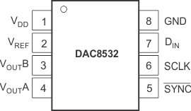
6 Pin Configuration and Functions

VSSOP (DGK) Package
8 Pins
Top View
pinout_SBAS246.gif

Pin Functions

PIN NAME FUNCTION
1 VDD Power supply input, 2.7 V to 5.5 V
2 VREF Reference voltage input
3 VOUTB Analog output voltage from DAC B
4 VOUTA Analog output voltage from DAC A
5 SYNC Level triggered SYNC input (active LOW). This is the frame synchronization signal for the input data. When SYNC goes LOW, it enables the input shift register and data is transferred on the falling edges of SCLK. The action specified by the 8-bit control byte and 16-bit data word is executed following the 24th falling SCLK clock edge (unless SYNC is taken HIGH before this edge in which case the rising edge of SYNC acts as an interrupt and the write sequence is ignored by the DAC8532).
6 SCLK Serial Clock Input. Data can be transferred at rates up to 30 MHz at 5 V.
7 DIN Serial Data Input. Data is clocked into the 24-bit input shift register on the falling edge of the serial clock input.
8 GND Ground reference point for all circuitry on the part.