ZHCSBK1C December   2006  – January 2018 DAC8560

PRODUCTION DATA.  

  1. 特性
  2. 应用
  3. 说明
    1.     Device Images
      1.      功能方框图
  4. 修订历史记录
  5. Pin Configuration and Functions
    1.     Pin Functions
  6. Specifications
    1. 6.1  Absolute Maximum Ratings
    2. 6.2  ESD Ratings
    3. 6.3  Recommended Operating Conditions
    4. 6.4  Thermal Information
    5. 6.5  Electrical Characteristics
    6. 6.6  Timing Requirements
    7. 6.7  Typical Characteristics: Internal Reference
    8. 6.8  Typical Characteristics: DAC at VDD = 5 V
    9. 6.9  Typical Characteristics: DAC at VDD = 3.6 V
    10. 6.10 Typical Characteristics: DAC at VDD = 2.7 V
  7. Detailed Description
    1. 7.1 Overview
    2. 7.2 Functional Block Diagram
    3. 7.3 Feature Description
      1. 7.3.1 Digital-to-Analog Converter (DAC)
      2. 7.3.2 Resistor String
      3. 7.3.3 Output Amplifier
      4. 7.3.4 DAC Noise Performance
      5. 7.3.5 Internal Reference
        1. 7.3.5.1 Enable/Disable Internal Reference
        2. 7.3.5.2 Internal Reference Load
          1. 7.3.5.2.1 Supply Voltage
          2. 7.3.5.2.2 Temperature Drift
          3. 7.3.5.2.3 Noise Performance
          4. 7.3.5.2.4 Load Regulation
          5. 7.3.5.2.5 Long-Term Stability
          6. 7.3.5.2.6 Thermal Hysteresis
    4. 7.4 Device Functional Modes
      1. 7.4.1 Power-Down Modes
    5. 7.5 Programming
      1. 7.5.1 Serial Interface
      2. 7.5.2 Input Shift Register
      3. 7.5.3 SYNC Interrupt
      4. 7.5.4 Power-On Reset
    6. 7.6 Register Maps
      1. 7.6.1 Write Sequence for Disabling the DAC8560 Internal Reference
        1. Table 1. Write Sequence for Disabling the DAC8560 Internal Reference
      2. 7.6.2 Enabling the DAC8560 Internal Reference (Write Sequence 1 of 2)
        1. Table 2. Enabling the DAC8560 Internal Reference (Write Sequence 1 of 2)
      3. 7.6.3 Enabling the DAC8560 Internal Reference (Write Sequence 2 of 2)
        1. Table 3. Enabling the DAC8560 Internal Reference (Write Sequence 2 of 2)
      4. 7.6.4 DAC8560 Data Input Register Format
        1. Table 4. DAC8560 Data Input Register Format
  8. Application and Implementation
    1. 8.1 Application Information
    2. 8.2 Typical Applications
      1. 8.2.1 Design Requirements
      2. 8.2.2 Detailed Design Procedure or Bipolar Operation > ±VREF
        1. 8.2.2.1 Bipolar Operation Greater Than ±VREF
          1. 8.2.2.1.1 Passive Component Selection
          2. 8.2.2.1.2 Amplifier Selection
        2. 8.2.2.2 Microprocessor Interfacing
          1. 8.2.2.2.1 DAC8560 to 8051 Interface
          2. 8.2.2.2.2 DAC8560 to Microwire Interface
          3. 8.2.2.2.3 DAC8560 to 68HC11 Interface
      3. 8.2.3 Application Curves
  9. Power Supply Recommendations
  10. 10Layout
    1. 10.1 Layout Guidelines
    2. 10.2 Layout Example
  11. 11器件和文档支持
    1. 11.1 文档支持
      1. 11.1.1 相关文档
    2. 11.2 接收文档更新通知
    3. 11.3 社区资源
    4. 11.4 商标
    5. 11.5 静电放电警告
    6. 11.6 术语表
  12. 12机械、封装和可订购信息

封装选项

机械数据 (封装 | 引脚)
散热焊盘机械数据 (封装 | 引脚)
订购信息

Typical Characteristics: Internal Reference

At TA = 25°C, unless otherwise noted.
DAC8560 tc_vref-tmp_cd_las464.gif
Figure 2. Internal Reference Voltage vs Temperature (Grades C and D)
DAC8560 tc_tmp_drift_cd_40_las464.gif
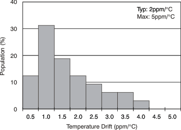
Figure 4. Reference Output Temperature Drift (–40°C to 120°C, Grades C and D)
DAC8560 tc_tmp_drift_cd_0_las464.gif
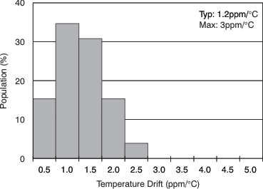
Figure 6. Reference Output Temperature Drift (0°C to 120°C, Grades C and D)
DAC8560 tc_ref_noise-freq_las464.gif
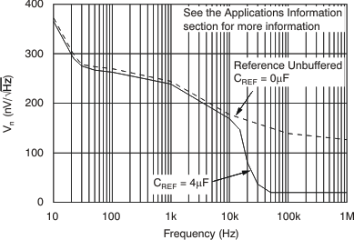
Explained in more detail in Application and Implementation.
Figure 8. Internal Reference Noise Density vs Frequency
DAC8560 tc_vref-iload_cd_las464.gif
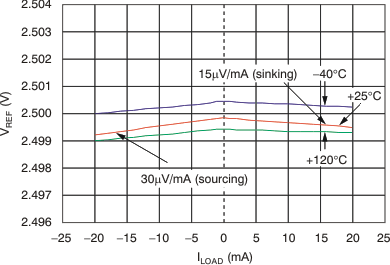
Figure 10. Internal Reference Voltage vs Load Current (Grades C and D)
DAC8560 tc_vref-vdd_cd_las464.gif
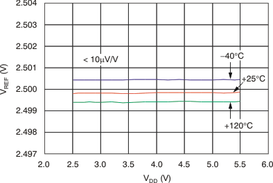
Figure 12. Internal Reference Voltage vs Supply Voltage (Grades C and D)
DAC8560 tc_vref-tmp_ab_las464.gif
Figure 3. Internal Reference Voltage vs Temperature (Grades A and B)
DAC8560 tc_temp_drift_ab_las464.gif
Figure 5. Reference Output Temperature Drift (–40°C to 120°, Grades A and B)
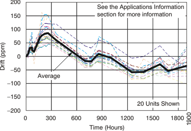
DAC8560 tc_long_term_drift_las464.gif
Explained in more detail in Application and Implementation .
Figure 7. Long-Term Stability/Drift (1)
DAC8560 tc_int_ref_noise_las464.gif
Explained in more detail in Application and Implementation.
Figure 9. Internal Reference Noise 0.1 Hz to 10 Hz
DAC8560 tc_vref-iload_ab_las464.gif
Figure 11. Internal Reference Voltage vs Load Current (Grades A and B)
DAC8560 tc_vref-vdd_ab_las464.gif
Figure 13. Internal Reference Voltage vs Supply Voltage (Grades A and B)