ZHCSBK1C December   2006  – January 2018 DAC8560

PRODUCTION DATA.  

  1. 特性
  2. 应用
  3. 说明
    1.     Device Images
      1.      功能方框图
  4. 修订历史记录
  5. Pin Configuration and Functions
    1.     Pin Functions
  6. Specifications
    1. 6.1  Absolute Maximum Ratings
    2. 6.2  ESD Ratings
    3. 6.3  Recommended Operating Conditions
    4. 6.4  Thermal Information
    5. 6.5  Electrical Characteristics
    6. 6.6  Timing Requirements
    7. 6.7  Typical Characteristics: Internal Reference
    8. 6.8  Typical Characteristics: DAC at VDD = 5 V
    9. 6.9  Typical Characteristics: DAC at VDD = 3.6 V
    10. 6.10 Typical Characteristics: DAC at VDD = 2.7 V
  7. Detailed Description
    1. 7.1 Overview
    2. 7.2 Functional Block Diagram
    3. 7.3 Feature Description
      1. 7.3.1 Digital-to-Analog Converter (DAC)
      2. 7.3.2 Resistor String
      3. 7.3.3 Output Amplifier
      4. 7.3.4 DAC Noise Performance
      5. 7.3.5 Internal Reference
        1. 7.3.5.1 Enable/Disable Internal Reference
        2. 7.3.5.2 Internal Reference Load
          1. 7.3.5.2.1 Supply Voltage
          2. 7.3.5.2.2 Temperature Drift
          3. 7.3.5.2.3 Noise Performance
          4. 7.3.5.2.4 Load Regulation
          5. 7.3.5.2.5 Long-Term Stability
          6. 7.3.5.2.6 Thermal Hysteresis
    4. 7.4 Device Functional Modes
      1. 7.4.1 Power-Down Modes
    5. 7.5 Programming
      1. 7.5.1 Serial Interface
      2. 7.5.2 Input Shift Register
      3. 7.5.3 SYNC Interrupt
      4. 7.5.4 Power-On Reset
    6. 7.6 Register Maps
      1. 7.6.1 Write Sequence for Disabling the DAC8560 Internal Reference
        1. Table 1. Write Sequence for Disabling the DAC8560 Internal Reference
      2. 7.6.2 Enabling the DAC8560 Internal Reference (Write Sequence 1 of 2)
        1. Table 2. Enabling the DAC8560 Internal Reference (Write Sequence 1 of 2)
      3. 7.6.3 Enabling the DAC8560 Internal Reference (Write Sequence 2 of 2)
        1. Table 3. Enabling the DAC8560 Internal Reference (Write Sequence 2 of 2)
      4. 7.6.4 DAC8560 Data Input Register Format
        1. Table 4. DAC8560 Data Input Register Format
  8. Application and Implementation
    1. 8.1 Application Information
    2. 8.2 Typical Applications
      1. 8.2.1 Design Requirements
      2. 8.2.2 Detailed Design Procedure or Bipolar Operation > ±VREF
        1. 8.2.2.1 Bipolar Operation Greater Than ±VREF
          1. 8.2.2.1.1 Passive Component Selection
          2. 8.2.2.1.2 Amplifier Selection
        2. 8.2.2.2 Microprocessor Interfacing
          1. 8.2.2.2.1 DAC8560 to 8051 Interface
          2. 8.2.2.2.2 DAC8560 to Microwire Interface
          3. 8.2.2.2.3 DAC8560 to 68HC11 Interface
      3. 8.2.3 Application Curves
  9. Power Supply Recommendations
  10. 10Layout
    1. 10.1 Layout Guidelines
    2. 10.2 Layout Example
  11. 11器件和文档支持
    1. 11.1 文档支持
      1. 11.1.1 相关文档
    2. 11.2 接收文档更新通知
    3. 11.3 社区资源
    4. 11.4 商标
    5. 11.5 静电放电警告
    6. 11.6 术语表
  12. 12机械、封装和可订购信息

封装选项

机械数据 (封装 | 引脚)
散热焊盘机械数据 (封装 | 引脚)
订购信息

Internal Reference

The DAC8560 includes a 2.5-V internal reference that is enabled by default. The internal reference is externally available at the VREF pin. TI recommends a minimum 100-nF capacitor between the reference output and GND for noise filtering.

The internal reference of the DAC8560 is a bipolar transistor-based, precision bandgap voltage reference. The basic bandgap topology is shown in Figure 65. Transistors Q1 and Q2 are biased such that the current density of Q1 is greater than that of Q2. The difference of the two base-emitter voltages (VBE1 – VBE2) has a positive temperature coefficient and is forced across resistor R1. This voltage is gained up and added to the base-emitter voltage of Q2, which has a negative temperature coefficient. The resulting output voltage is virtually independent of temperature. The short-circuit current is limited by design to approximately 100 mA.
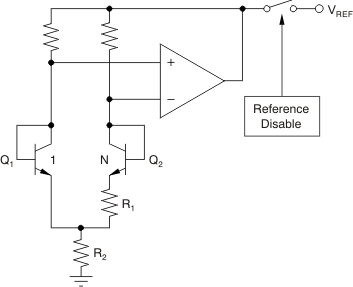
DAC8560 too_bandgap_las464.gifFigure 65. Simplified Schematic of the Bandgap Reference