ZHCSBK1C December 2006 – January 2018 DAC8560
PRODUCTION DATA.
- 1 特性
- 2 应用
- 3 说明
- 4 修订历史记录
- 5 Pin Configuration and Functions
-
6 Specifications
- 6.1 Absolute Maximum Ratings
- 6.2 ESD Ratings
- 6.3 Recommended Operating Conditions
- 6.4 Thermal Information
- 6.5 Electrical Characteristics
- 6.6 Timing Requirements
- 6.7 Typical Characteristics: Internal Reference
- 6.8 Typical Characteristics: DAC at VDD = 5 V
- 6.9 Typical Characteristics: DAC at VDD = 3.6 V
- 6.10 Typical Characteristics: DAC at VDD = 2.7 V
-
7 Detailed Description
- 7.1 Overview
- 7.2 Functional Block Diagram
- 7.3 Feature Description
- 7.4 Device Functional Modes
- 7.5 Programming
- 7.6 Register Maps
- 8 Application and Implementation
- 9 Power Supply Recommendations
- 10Layout
- 11器件和文档支持
- 12机械、封装和可订购信息
8.2.2.2.1 DAC8560 to 8051 Interface
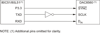
See Figure 73 for a serial interface between the DAC8560 and a typical 8051-type microcontroller. The setup for the interface is as follows: TXD of the 8051 drives SCLK of the DAC8560, while RXD drives the serial data line of the device. The SYNC signal is derived from a bit-programmable pin on the port of the 8051. In this case, port line P3.3 is used. When data is to be transmitted to the DAC8560, P3.3 is taken LOW. The 8051 transmits data in 8-bit bytes; thus, only eight falling clock edges occur in the transmit cycle. To load data to the DAC, P3.3 is left LOW after the first eight bits are transmitted, then a second write cycle is initiated to transmit the second byte of data. P3.3 is taken HIGH following the completion of the third write cycle. The 8051 outputs the serial data in a format which has the LSB first. The DAC8560 requires its data with the MSB as the first bit received. The 8051 transmit routine must therefore take this into account, and mirror the data as needed.
 Figure 73. DAC8560 to 80C51/80L51 Interface