ZHCSC70D December 2013 – December 2021 DAC7750 , DAC8750
PRODUCTION DATA
- 1 特性
- 2 应用
- 3 说明
- 4 Revision History
- 5 Device Comparison Table
- 6 Pin Configuration and Functions
- 7 Specifications
- 8 Detailed Description
- 9 Application and Implementation
- 10Power Supply Recommendations
- 11Layout
- 12Device and Documentation Support
- 13Mechanical, Packaging, and Orderable Information
封装选项
机械数据 (封装 | 引脚)
散热焊盘机械数据 (封装 | 引脚)
订购信息
9.2.2 Detailed Design Procedure
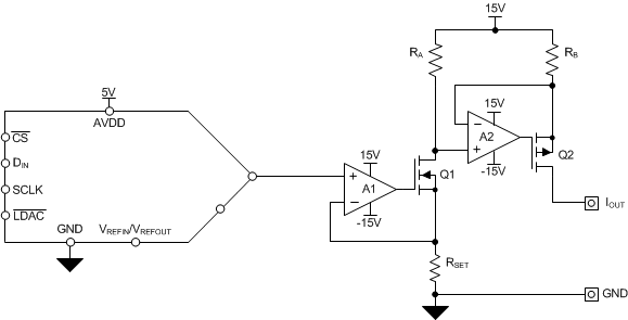
Figure 9-4 illustrates a common generic solution for realizing these desired voltage and current output spans.
 Figure 9-4 Generic
Design for Typical PLC Current and Voltage Outputs
Figure 9-4 Generic
Design for Typical PLC Current and Voltage OutputsThe current output circuit is comprised of amplifiers A1 and A2, MOSFETs Q1 and Q1, and the three resistors RSET, RA, and RB. This two-stage current source enables the ground-referenced DAC output voltage to drive the high-side amplifier required for the current-source.
The high-level of integration of the DACx750 family lends itself very well to the design of analog output modules, offering simplicity of design and reducing solution size. The DACx750 integrates all of the components shown in Figure 9-4 allowing a software configurable current output driver. Figure 9-3 illustrates an example circuit design for such an application using the DACx750 for the current output driver.
The design uses two triple channel isolators (ISO7631FC) to provide galvanic isolation for the digital lines to communicate to the main controller. Note that these isolators can be driven by the internally-generated supply (DVDD) from the DACx750 to save components and cost. The DACx750 supplies up to 10 mA that meets the supply requirements of the two isolators running at up to 10 Mbps. Note that additional cost savings are possible if noncritical digital signals such as CLR and ALARM are tied to GND or left unconnected. Finally, a protection scheme with transient voltage suppressors and other components is placed on all pins which connect to the field.
The protection circuitry is designed to provide immunity to the IEC61000-4 test suite which includes system-level industrial transient tests. The protection circuit includes transient voltage suppressor (TVS) diodes, clamp-to-rail steering diodes, and pass elements in the form of resistors and ferrite beads. For more detail about selecting these components, see the Single-Channel Industrial Voltage and Current Output Driver, Isolated, EMC/EMI Tested Reference Design.