ZHCSC70D December 2013 – December 2021 DAC7750 , DAC8750
PRODUCTION DATA
- 1 特性
- 2 应用
- 3 说明
- 4 Revision History
- 5 Device Comparison Table
- 6 Pin Configuration and Functions
- 7 Specifications
- 8 Detailed Description
- 9 Application and Implementation
- 10Power Supply Recommendations
- 11Layout
- 12Device and Documentation Support
- 13Mechanical, Packaging, and Orderable Information
封装选项
机械数据 (封装 | 引脚)
散热焊盘机械数据 (封装 | 引脚)
订购信息
8.3.11 Programmable Slew Rate
The slew rate control feature controls the rate at which the output current changes. With the slew rate control feature disabled, the output changes smoothly at a rate limited by the output drive circuitry and the attached load.
To reduce the slew rate, enable the slew rate control feature through bit 4 of the Control Register. With this feature enabled, the output does not slew directly between the two values. Instead, the output steps digitally at a rate defined by bits [7:5] (SRSTEP) and bits [11:8] (SRCLK) of the Control Register. SRCLK defines the rate at which the digital slew updates, and SRSTEP defines the amount by which the output value changes at each update. If the DAC data register is read while the DAC output is still changing, the instantaneous value is read. Table 8-3 lists the slew rate step-size options. Table 8-4 summarizes the slew rate update clock options.
| SRSTEP | STEP SIZE (LSB) | |
|---|---|---|
| DAC7750 | DAC8750 | |
| 000 | 0.0625 | 1 |
| 001 | 0.125 | 2 |
| 010 | 0.25 | 4 |
| 011 | 0.5 | 8 |
| 100 | 1 | 16 |
| 101 | 2 | 32 |
| 110 | 4 | 64 |
| 111 | 8 | 128 |
| SRCLK | DAC UPDATE FREQUENCY (Hz) |
|---|---|
| 0000 | 258,065 |
| 0001 | 200,000 |
| 0010 | 153,845 |
| 0011 | 131,145 |
| 0100 | 115,940 |
| 0101 | 69,565 |
| 0110 | 37,560 |
| 0111 | 25,805 |
| 1000 | 20,150 |
| 1001 | 16,030 |
| 1010 | 10,295 |
| 1011 | 8,280 |
| 1100 | 6,900 |
| 1101 | 5,530 |
| 1110 | 4,240 |
| 1111 | 3,300 |
The time required for the output to slew over a given range is expressed as Equation 5.

where
- Slew Time is expressed in seconds
- Output Change is expressed in amps (A) for IOUT or volts (V) for VOUT
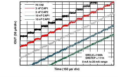
When the slew rate control feature is enabled, all output changes happen at the programmed slew rate. This configuration results in a staircase formation at the output. If the CLR pin is asserted, the output slews to the zero-scale value at the programmed slew rate. Read bit 1 (SR-ON) of the Status Register to verify that the slew operation has completed. The update clock frequency for any given value is the same for all output ranges. The step size, however, varies across output ranges for a given value of step size because the LSB size is different for each output range. Figure 8-4 shows an example of IOUT slewing at a rate set by the previously described parameters. In this example for the DAC8750 (LSB size of 305 nA for the 0-mA to 20-mA range), the settings correspond to an update clock frequency of 6.9 kHz and a step size of 128 LSB. As shown in the case with no capacitors on CAP1 or CAP2, the steps occur at the update clock frequency (6.9 kHz corresponds to a period close to 150 µs), and the size of each step is approximately 38 µA (128 × 305 nA). Calculate the slew time for a specific code change by using Equation 5.
 Figure 8-4 IOUT vs Time With Digital Slew Rate
Control
Figure 8-4 IOUT vs Time With Digital Slew Rate
ControlApply the desired programmable slew rate control setting before updating the DAC data register because updates to the DAC data register in tandem with updates to the slew rate control registers can create race conditions that may result in unexpected DAC data.