ZHCSHP3 February 2018 DAC8771
PRODUCTION DATA.
- 1 特性
- 2 应用
- 3 说明
- 4 修订历史记录
- 5 Device Comparison Table
- 6 Pin Configuration and Functions
- 7 Specifications
-
8 Detailed Description
- 8.1 Overview
- 8.2 Functional Block Diagram
- 8.3
Feature Description
- 8.3.1 Current Output Stage
- 8.3.2 Voltage Output Stage
- 8.3.3 Buck-Boost Converter
- 8.3.4 Analog Power Supply
- 8.3.5 Digital Power Supply
- 8.3.6 Internal Reference
- 8.3.7 Power-On-Reset
- 8.3.8 ALARM Pin
- 8.3.9 Power GOOD bit
- 8.3.10 Status Register
- 8.3.11 Status Mask
- 8.3.12 Alarm Action
- 8.3.13 Watchdog Timer
- 8.3.14 Programmable Slew Rate
- 8.3.15 HART Interface
- 8.4 Device Functional Modes
- 8.5
Register Maps
- 8.5.1
Register Maps
- 8.5.1.1 DAC8771 Commands
- 8.5.1.2
Register Maps and Bit Functions
- 8.5.1.2.1 No Operation Register (address = 0x00) [reset = 0x0000]
- 8.5.1.2.2 Reset Register (address = 0x01) [reset = 0x0000]
- 8.5.1.2.3 Reset Config Register (address = 0x02) [reset = 0x0000]
- 8.5.1.2.4 Select DAC Register (address = 0x03) [reset = 0x0000]
- 8.5.1.2.5 Configuration DAC Register (address = 0x04) [reset = 0x0000]
- 8.5.1.2.6 DAC Data Register (address = 0x05) [reset = 0x0000]
- 8.5.1.2.7 Select Buck-Boost Converter Register (address = 0x06) [reset = 0x0000]
- 8.5.1.2.8 Configuration Buck-Boost Register (address = 0x07) [reset = 0x0000]
- 8.5.1.2.9 DAC Channel Calibration Enable Register (address = 0x08) [reset = 0x0000]
- 8.5.1.2.10 DAC Channel Gain Calibration Register (address = 0x09) [reset = 0x0000]
- 8.5.1.2.11 DAC Channel Offset Calibration Register (address = 0x0A) [reset = 0x0000]
- 8.5.1.2.12 Status Register (address = 0x0B) [reset = 0x1000]
- 8.5.1.2.13 Status Mask Register (address = 0x0C) [reset = 0x0000]
- 8.5.1.2.14 Alarm Action Register (address = 0x0D) [reset = 0x0000]
- 8.5.1.2.15 User Alarm Code Register (address = 0x0E) [reset = 0x0000]
- 8.5.1.2.16 Reserved Register (address = 0x0F) [reset = N/A]
- 8.5.1.2.17 Write Watchdog Timer Register (address = 0x10) [reset = 0x0000]
- 8.5.1.2.18 Reserved Register (address 0x12 - 0xFF) [reset = N/A]
- 8.5.1
Register Maps
- 9 Application and Implementation
- 10Power Supply Recommendations
- 11Layout
- 12器件和文档支持
- 13机械、封装和可订购信息
9.1.1 Buck-Boost Converter External Component Selection
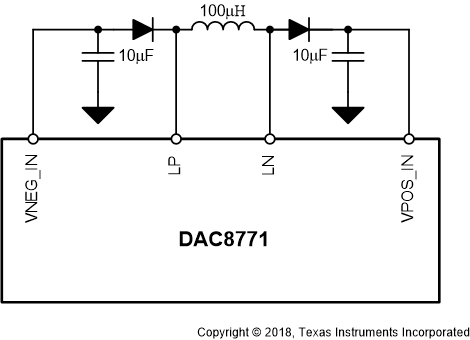
 Figure 122. DAC8771 External Buck-Boost Components with Recommended Values
The buck-boost converter integrated in the DAC8771 requires three external passive components for operation: a single inductor along with two storage capacitors and two switching diodes, one for each VPOS_IN and VNEG_IN when active. If only one output is used, either VPOS_IN or VNEG_IN, the inactive output components may be removed and the respective inputs tied to ground. In order to meet the parametric performance outlined in the section for the voltage output, 500 mV of footroom is required on VNEG_IN.
The recommended value for the external inductor is 100 µH with at least 500 mA peak inductor current. Reducing the inductor value to as low as 80 µH is possible, though this will limit the buck-boost converter maximum input voltage to output voltage ratio, reduce efficiency, and increase ripple. Reducing the inductor below 80 µH will result in device damage. Peak inductor current should be rated at 500 mA or greater with 20% inductance tolerance at peak current. If peak inductor current for an inductor is violated the effective inductance is reduced, which will impact maximum input to output voltage ratio, efficiency, and ripple.
An output, or storage, X7R capacitor with value of 10 µF and voltage rating of 50 V is recommended though other values and dielectric materials may be used without damaging the DAC8771. Reducing capacitor value will increase buck-boost converter output ripple and reduced voltage rating will reduce effective capacitance at full-scale buck-boost converter outputs. X7R capacitors are rated for –55°C to 125°C operation with 15% maximum capacitance variance over temperature. Designs operating over reduced temperature spans and with loose efficiency requirements may use different dielectric material. C0G capacitor typically offer tighter capacitance variance but come in larger packages, but may be beneficial substitutes.
The external diode switches illustrated on the left and right side of the 100 µH inductor shown in Figure 122 should be selected based on reverse voltage rating, reverse recovery time, leakage or parasitic capacitance, and current or power ratings. Breakdown voltage rating of at least 60 V is recommended to accommodate for the maximum voltage that may be across the diode when both VPOS and VNEG are both active during switching of the DC/DC. Minimal reverse recovery time and parasitic capacitance is recommended in order to preserve efficiency of the DC/DC. The external diode should be rated for at least 500 mA average forward current.