ZHCSFZ2 February 2017 DAC8775
PRODUCTION DATA.
- 1 特性
- 2 应用范围
- 3 说明
- 4 修订历史记录
- 5 Device Comparison Table
- 6 Pin Configuration and Functions
- 7 Specifications
-
8 Detailed Description
- 8.1 Overview
- 8.2 Functional Block Diagram
- 8.3
Feature Description
- 8.3.1 Current Output Stage
- 8.3.2 Voltage Output Stage
- 8.3.3 Buck-Boost Converter
- 8.3.4 Analog Power Supply
- 8.3.5 Digital Power Supply
- 8.3.6 Internal Reference
- 8.3.7 Power-On-Reset
- 8.3.8 ALARM Pin
- 8.3.9 Power GOOD Bits
- 8.3.10 Status Register
- 8.3.11 Status Mask
- 8.3.12 Alarm Action
- 8.3.13 Watchdog Timer
- 8.3.14 Programmable Slew Rate
- 8.3.15 HART Interface
- 8.4 Device Functional Modes
- 8.5
Register Maps
- 8.5.1 DAC8775 Commands
- 8.5.2
Register Maps and Bit Functions
- 8.5.2.1 No Operation Register (address = 0x00) [reset = 0x0000]
- 8.5.2.2 Reset Register (address = 0x01) [reset = 0x0000]
- 8.5.2.3 Reset Config Register (address = 0x02) [reset = 0x0000]
- 8.5.2.4 Select DAC Register (address = 0x03) [reset = 0x0000]
- 8.5.2.5 Configuration DAC Register (address = 0x04) [reset = 0x0000]
- 8.5.2.6 DAC Data Register (address = 0x05) [reset = 0x0000]
- 8.5.2.7 Select Buck-Boost Converter Register (address = 0x06) [reset = 0x0000]
- 8.5.2.8 Configuration Buck-Boost Register (address = 0x07) [reset = 0x0000]
- 8.5.2.9 DAC Channel Calibration Enable Register (address = 0x08) [reset = 0x0000]
- 8.5.2.10 DAC Channel Gain Calibration Register (address = 0x09) [reset = 0x0000]
- 8.5.2.11 DAC Channel Offset Calibration Register (address = 0x0A) [reset = 0x0000]
- 8.5.2.12 Status Register (address = 0x0B) [reset = 0x1000]
- 8.5.2.13 Status Mask Register (address = 0x0C) [reset = 0x0000]
- 8.5.2.14 Alarm Action Register (address = 0x0D) [reset = 0x0000]
- 8.5.2.15 User Alarm Code Register (address = 0x0E) [reset = 0x0000]
- 8.5.2.16 Reserved Register (address = 0x0F) [reset = N/A]
- 8.5.2.17 Write Watchdog Timer Register (address = 0x10) [reset = 0x0000]
- 8.5.2.18 Device ID Register (address = 0x11) [reset = 0x0000]
- 8.5.2.19 Reserved Register (address 0x12 - 0xFF) [reset = N/A]
- 9 Application and Implementation
- 10Power Supply Recommendations
- 11Layout
- 12器件和文档支持
- 13机械、封装和可订购信息
9 Application and Implementation
NOTE
Information in the following applications sections is not part of the TI component specification, and TI does not warrant its accuracy or completeness. TI’s customers are responsible for determining suitability of components for their purposes. Customers should validate and test their design implementation to confirm system functionality.
9.1 Application Information
9.1.1 Buck-Boost Converter External Component Selection
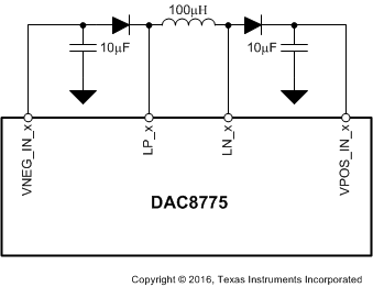 Figure 127. DAC8775 External Buck-Boost Components with Recommended Values
The buck-boost converters integrated in the DAC8775 each require three external passive components for operation: a single inductor per channel as well as storage capacitors and switching diodes for each VPOS_IN_x and VNEG_IN_x channels that are active. If only one output is used, either VPOS_IN_x or VNEG_IN_x, the inactive output components may be removed and the respective inputs tied to ground. In order to meet the parametric performance outlined in the Electrical Characteristics section for the voltage output, 500 mV of foot-room is required on VNEG_IN_x.
The recommended value for the external inductor is 100 µH with at least 500 mA peak inductor current. Reducing the inductor value to as low as 80 µH is possible, though this will limit the buck-boost converter maximum input voltage to output voltage ratio, reduce efficiency, and increase ripple. Reducing the inductor below 80 µH will result in device damage. Peak inductor current should be rated at 500 mA or greater with 20% inductance tolerance at peak current. If peak inductor current for an inductor is violated the effective inductance is reduced, which will impact maximum input to output voltage ratio, efficiency, and ripple.
An output, or storage, X7R capacitor with value of 10 µF and voltage rating of 50 V is recommended though other values and dielectric materials may be used without damaging the DAC8775. Reducing capacitor value will increase buck-boost converter output ripple and reduced voltage rating will reduce effective capacitance at full-scale buck-boost converter outputs. X7R capacitors are rated for –55°C to 125°C operation with 15% maximum capacitance variance over temperature. Designs operating over reduced temperature spans and with loose efficiency requirements may use different dielectric material. C0G capacitor typically offer tighter capacitance variance but come in larger packages, but may be beneficial substitutes.
The external diode switches illustrated on the left and right side of the 100 µH inductor shown in Figure 127 should be selected based on reverse voltage rating, reverse recovery time, leakage or parasitic capacitance, and current or power ratings. Breakdown voltage rating of at least 60 V is recommended to accommodate for the maximum voltage that may be across the diode when both VPOS_x and VNEG_x are both active during switching of the DC/DCs. Minimal reverse recovery time and parasitic capacitance is recommended in order to preserve efficiency of the DC/DCs. The external diode should be rated for at least 500 mA average forward current.
9.1.2 Voltage and Current Ouputs on a Shared Terminal
Figure 128 illustrates a simplified block diagram of the voltage output stages of the DAC8775.
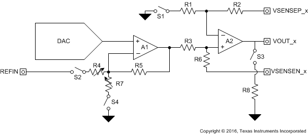 Figure 128. Simplified Block Diagram of Voltage Output Architecture
When designing for a shared voltage and current output terminal it is important to consider leakage paths that may corrupt the voltage or current output stages.
When the voltage output is active and the current output is inactive the IOUT_x pin becomes a high-impedance node and therefore does not significantly load the voltage output in a way that would degrade VOUT_x performance. When the voltage output is inactive and the current output is active switches S1, S2, and S4 all become open while switch S3 is controlled by the POC bit in the Reset Config Register for each respective channel. When the POC bit is set to a 0, the default value, switch S3 is closed when VOUT is disabled. This creates a leakage path with respect to the current output when the terminals are shared which will create a load-dependent error. In order to reduce this error the POC bit can be set to a 1 which opens switch S3, effectively making the VOUT pin high-impedance and reducing the magnitude of leakage current.
9.1.3 Optimizing Current Output Settling time with Auto learn Mode
When the buck-boost converters are active power and heat dissipation of the device are at a minimum, however settling time of the current output is dominated by the slew rate of the buck-boost converter, which is significantly slower that the current output signal chain alone. When the buck-boost converters are bypassed settling time of the current output is minimized while power and heat dissipation are significant.
Auto-learn mode offers an alternative mode which allows the buck-boost converter to learn the size of the load and choose a clamped output value that does not change over the full range of the selected current output. This allows a balance between settling time and power dissipation. There are two options for entering auto-learn mode:
- Enable the buck-boost converter in full-tracking mode followed by enabling the current output. Until the DAC code 0x4000 is passed, settling time will be dominated by the buck-boost converter. After code 0x400 is surpassed the buck-boost converter detects the load and sets the clamp value appropriately.
- Enable the buck-boost converter in clamp-mode with clamp value set to a greater voltage than required by the largest load the current output will be expected to drive, followed by enabling the current output. Enter full-tracking mode. In this case the clamp value of maintained without the buck-boost converter output changing, therefore settling time is set by the IOUT_x signal chain. After code 0x4000 is surpassed the buck-boost converter detects the load and adjusts the clamp value appropriately. At all times using this initialization procedure the settling time is defined by the IOUT_x signal chain.
9.1.4 Protection for Industrial Transients
In order to successfully protect the DAC8775, or any integrated circuit, against industrial transient testing the internal structures and how they may behave when exposed to said signals must be understood. Figure 129 depicts a simplified representation of internal structures present on the device’s output pins which are represented as a pair of clamp-to-rail diodes connected to the VPOS_IN_x and VNEG_IN_x supply rails.
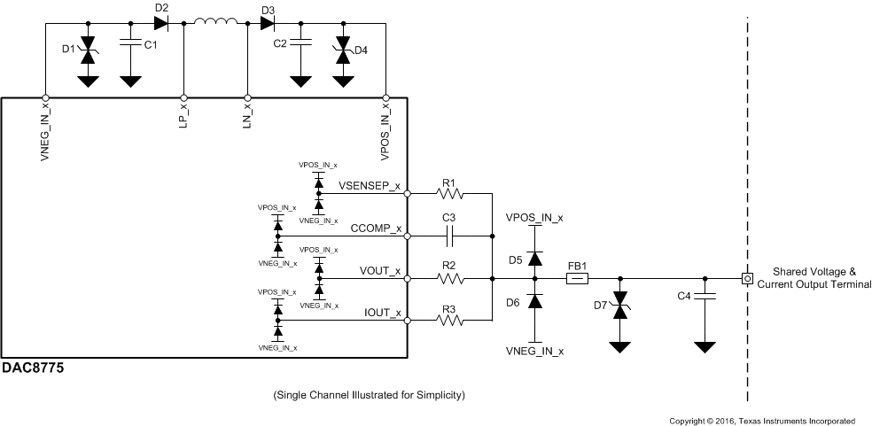 Figure 129. Simplified Block Diagram of Internal Structures and External Protection
When these internal structures are exposed to industrial transient testing, without the external protection components, the diode structures will become forward biased and conduct current. If the conducted current is too large, which is often true for high-voltage industrial transient tests, the structures will become permanently damaged and impact device functionality.
Both attenuation and diversion strategies are implemented to protect the internal structures as well as the device itself. Attenuation is realized by capacitor C4 which forms an R/C low-pass filter when interacting with the source impedance of the transient generator, ferrite bead FB1 also helps attenuate high-frequency current, along with both AC and DC current limiters realized by series pass elements R1, R2, and R3. Diversion is achieved by transient voltage suppressor (TVS) diode D7 and clamp-to-rail diodes D5 and D6. The combined effects of both strategies effectively limit the current flowing into the device and through the internal diode structures such that the device is not damaged and remains functional.
It is important to also include TVS diodes D1 and D4 at the VPOS_IN_x and VNEG_IN_x nodes in order to provide a discharge path for the energy that is going to be sent to these nodes through diodes D5, D6, and the internal diode structures. Without these diodes when current is diverted to these nodes the DC/DC converter storage capacitors C1 and C2 will charge, slowly increasing the voltage at these nodes.
9.1.5 Implementing HART with DAC8775
The DAC8775 features internal resistors to convert a 500-mVpp HART FSK signal sourced by an external HART modem. These resistors are ratiometrically matched to the gain-setting resistors for the current output signal chain to ensure that a 500-mVpp input at the HART_IN_x pin is delivered as a 1-mApp signal at the respective IOUT_x pin regardless of which gain mode is selected.
An external capacitor, placed in series between the HART_IN_x pin and HART FSK source, is required to AC couple the HART FSK signal to the HART_IN_x pin. The recommended capacitance for this external capacitor is from 10 nF to 22 nF.
9.2 Typical Application
9.2.1 1W Power Dissipation, Quad Channel, EMC and EMI Protected Analog Output Module with Adaptive Power Management
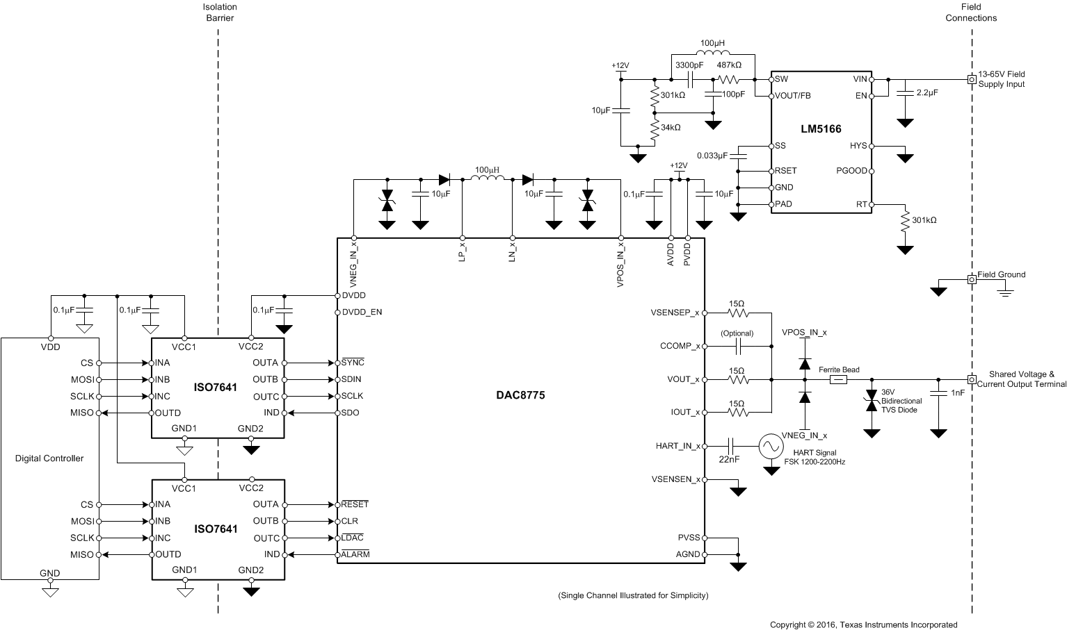 Figure 130. DAC8775 in Quad-Channel PLC AO Module
9.2.2 Design Requirements
Analog I/O modules are used by programmable logic controllers (PLCs) to interface sensors, actuators, and other field instruments. These modules must meet stringent electrical specifications for both accuracy and robust protection. These outputs are typically current outputs based on the 4-mA to 20-mA range and derivatives or voltage outputs ranging from 0 V to 5 V, 0 V to 10 V, ±5 V, and ±10 V. Common error budgets accommodate 0.1% full-scale range total unadjusted error (% FSR TUE) at room temperature. Designs that desire stronger accuracy over temperature frequently implement calibration. Often the PLC back-plane provides access to a 12-V to 36-V analog supply from which a majority of analog supply voltages are derived.
Analog output modules are frequently multi-channel modules featuring either channel-to-channel isolation between each channel or group isolation where several channels share a common ground connection. As channel count increases it is desirable to maintain small form-factor requiring high levels of integration and reduced power dissipation in order to control heat inside of the PLC enclosure.
Therefore the design requirements are:
- Support of standard industrial automation voltage and current output spans
- Operation with standard industrial automation supply voltages from 12 V to 36 V
- Current and voltage outputs with TUE less than 0.1% at 25°C
- Total on-board power dissipation less than or equal to 1 W
- At minimum criteria B IEC61000-4 ESD, EFT, CI, and Surge immunity
9.2.3 Detailed Design Procedure
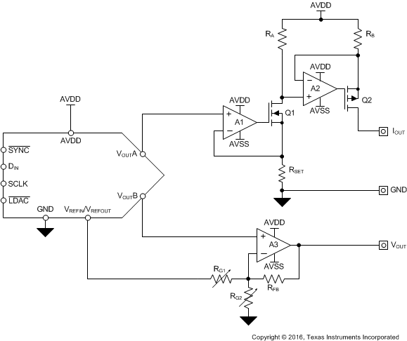 Figure 131. Generic Design for Typical PLC Current and Voltage Outputs
Figure 131 illustrates a common generic solution for realizing the desired voltage and current output spans for industrial automation applications.
The current output circuit is comprised of amplifiers A1 and A2, MOSFETs Q1 and Q2, and the three resistors RSET, RA, and RB. This two-stage current source enables the ground-referenced DAC output voltage to drive the high-side amplifier required for the current-source.
The voltage output circuit is composed of amplifier A3 and the resistor network consisting of RFB, RG1, and RG2. A3 operates as a modified summing amplifier, where the DAC controls the non-inverting input and inverting input has one path to GND and a second to VREF. This configuration allows the single-ended DAC to create both the unipolar 0-V to 5-V and 0-V to 10-V outputs and the bipolar ±5-V and ±10-V outputs by modifying the values of RG1 and RG2.
Though this generic circuit realizes the desired spans, both the voltage and current outputs have short-comings. The current output high-side supply voltage is typically 24 V, when driving low impedance loads with this supply voltage a considerable amount of power is dissipated on RB and Q2. This power dissipation results in increased heat which leads to drift errors for amplifiers A1 and A2 as well as the DAC, resistors, and the reference voltage. In order to reduce the power dissipation in the high-side voltage to current converter circuit a feedback system which monitors the voltage drop across Q2 and adaptively adjusts the high-side supply voltage can be implemented. This feedback system adjusts the high side supply voltage to the minimum supply required to keep Q2 in the linear region of operation, avoiding compliance voltage saturation, reducing power dissipation and heat to a minimum which helps maintain accuracy.
The generic voltage output circuit performs well but does not compensate for errors associated with excessive output impedance or differences in ground potential from the local PLC ground and the load ground. A modified circuit can be implemented which provides connections to sense errors associated with both output impedance voltage drops and differences in ground potentials, this circuit is shown in Figure 128.
Figure 130 illustrates the DAC8775 along with the LM5166 in a quad-channel PLC analog output module. The DAC8775 includes the generic voltage and current output circuits along with buck-boost converter and feedback circuits for the current output and positive and negative sense connections for the voltage output circuit. The DAC8775 includes an internal reference and internal LDO for supplying the field-side of a digital isolator along with the buck-boost converter generating the single or dual high voltage supplies required for the output circuits, all powered from a single supply.
The DAC8775 buck-boost converter operates at peak efficiency with 12-V input voltage with peak power consumption of approximately 780mW. The LM5166 circuit accepts a wide range of input voltages from just above 12 V to 65 V, providing coverage for most standard PLC supply voltages, and buck-converts this supply voltage to the optimal 12-V supply for the DAC8775. Cumulative power dissipation for the DAC8775 and LM5166 is under 1 W.
Two ISO7641 devices implement galvanic isolation for all of the digital communication lines, though only a single ISO7641 is required for basic communication with the DAC8775 SPI compatible interface. An output protection circuit is included which is designed to provide immunity to the IEC61000-4 industrial transient and radiation test suite. The protection circuit includes transient voltage suppressor (TVS) diodes, clamp-to-rail steering diodes, and pass elements in the form of resistors and ferrite beads.
9.2.4 Application Curves
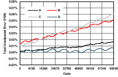 Figure 132. 4-mA to 20-mA IOUT TUE vs Code
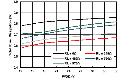 Figure 134. Total On-Board Power Dissipation vs Supply
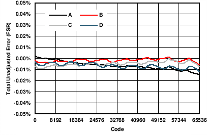 Figure 133. ±10-V VOUT TUE vs Code