ZHCSFZ2 February 2017 DAC8775
PRODUCTION DATA.
- 1 特性
- 2 应用范围
- 3 说明
- 4 修订历史记录
- 5 Device Comparison Table
- 6 Pin Configuration and Functions
- 7 Specifications
-
8 Detailed Description
- 8.1 Overview
- 8.2 Functional Block Diagram
- 8.3
Feature Description
- 8.3.1 Current Output Stage
- 8.3.2 Voltage Output Stage
- 8.3.3 Buck-Boost Converter
- 8.3.4 Analog Power Supply
- 8.3.5 Digital Power Supply
- 8.3.6 Internal Reference
- 8.3.7 Power-On-Reset
- 8.3.8 ALARM Pin
- 8.3.9 Power GOOD Bits
- 8.3.10 Status Register
- 8.3.11 Status Mask
- 8.3.12 Alarm Action
- 8.3.13 Watchdog Timer
- 8.3.14 Programmable Slew Rate
- 8.3.15 HART Interface
- 8.4 Device Functional Modes
- 8.5
Register Maps
- 8.5.1 DAC8775 Commands
- 8.5.2
Register Maps and Bit Functions
- 8.5.2.1 No Operation Register (address = 0x00) [reset = 0x0000]
- 8.5.2.2 Reset Register (address = 0x01) [reset = 0x0000]
- 8.5.2.3 Reset Config Register (address = 0x02) [reset = 0x0000]
- 8.5.2.4 Select DAC Register (address = 0x03) [reset = 0x0000]
- 8.5.2.5 Configuration DAC Register (address = 0x04) [reset = 0x0000]
- 8.5.2.6 DAC Data Register (address = 0x05) [reset = 0x0000]
- 8.5.2.7 Select Buck-Boost Converter Register (address = 0x06) [reset = 0x0000]
- 8.5.2.8 Configuration Buck-Boost Register (address = 0x07) [reset = 0x0000]
- 8.5.2.9 DAC Channel Calibration Enable Register (address = 0x08) [reset = 0x0000]
- 8.5.2.10 DAC Channel Gain Calibration Register (address = 0x09) [reset = 0x0000]
- 8.5.2.11 DAC Channel Offset Calibration Register (address = 0x0A) [reset = 0x0000]
- 8.5.2.12 Status Register (address = 0x0B) [reset = 0x1000]
- 8.5.2.13 Status Mask Register (address = 0x0C) [reset = 0x0000]
- 8.5.2.14 Alarm Action Register (address = 0x0D) [reset = 0x0000]
- 8.5.2.15 User Alarm Code Register (address = 0x0E) [reset = 0x0000]
- 8.5.2.16 Reserved Register (address = 0x0F) [reset = N/A]
- 8.5.2.17 Write Watchdog Timer Register (address = 0x10) [reset = 0x0000]
- 8.5.2.18 Device ID Register (address = 0x11) [reset = 0x0000]
- 8.5.2.19 Reserved Register (address 0x12 - 0xFF) [reset = N/A]
- 9 Application and Implementation
- 10Power Supply Recommendations
- 11Layout
- 12器件和文档支持
- 13机械、封装和可订购信息
11 Layout
11.1 Layout Guidelines
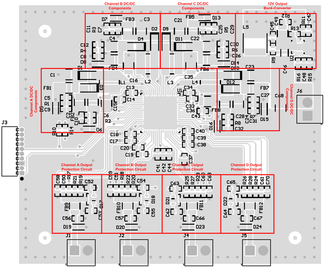
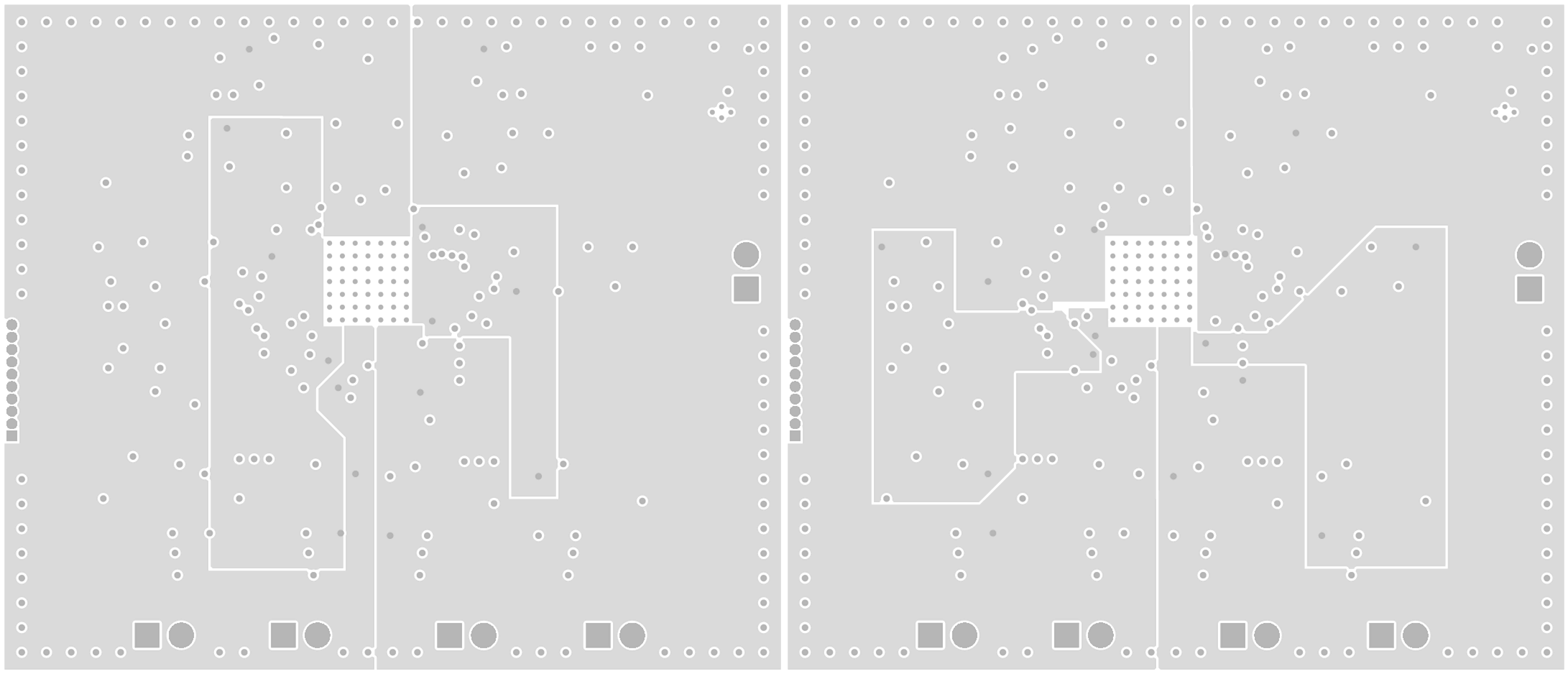
An example layout based on the design discussed in the Typical Application section is shown in the Layout Example section. Figure 139 shows the top-layer of the design which illustrates all component placement as no components are placed on the bottom layer. Figure 140 shows two of the internal power-layers: the layer on the left contains VPOS_IN_B, VPOS_IN_C, VNEG_IN_B, and VNEG_IN_D nets while the layer on the right contains VPOS_IN_A, VPOS_IN_D, VNEG_IN_A, and VNEG_IN_C nets.
The layer stack-up for this 6-layer example layout is shown below. A 6-layer design is not required, however provides optimal conditions for ground and power-supply planes. The solid ground plane beneath the majority of the signal traces, which are placed on the top layer, allows for a clean return path for sensitive analog traces and keeps them isolated from the internal power supply nets which will exhibit ripple from the DC/DC converter.
 Figure 138. Example Layout Layer Stack-Up
Traces for the DC/DC external components should be as low impedance, low inductance, and low capacitance as possible in order to maintain optimum performance. As such wide traces should be used to minimize inductance with minimal use of vias as vias will contribute large inductance and capacitance to the trace. For this reason it is recommended that all DC/DC components placed on the top layer.
The industrial transient protection circuit should be placed as close to the output connectors as possible to ensure that the return currents from these transients have a controlled path to exit the PCB which does not impact the analog circuitry.
Split ground planes for the DC/DC, digital, and analog grounds are not required but may be helpful to isolated ground return currents from cross-talk. If split ground planes are used care should be taken to ensure that signal traces are only placed above or below the locations where their respective grounds are placed in order to mitigate unexpected return paths or coupling to the other ground planes. If a single ground plane is used it is advisable to follow similar practices implementing a star-ground where the respective return currents interact with one another minimally. The example layout uses a single ground plane, based on measured results, performs similarly to an identical version with split ground planes.
The perimeter of the board is stitched with vias in order to enhance design performance against environments which may include radiated emissions. Additional vias are placed in critical areas nearby the design in order to place ground pours in between nodes to reduce cross-talk between adjacent traces.
Standard best-practices should be applied to the remaining components, including but not limited to, placing decoupling capacitors close to their respective pins and using wide traces or copper pours where possible, particularly for power traces where high current may flow.
11.2 Layout Example
 Figure 139. Application Example Layout
 Figure 140. Example Design Internal Copper Pours